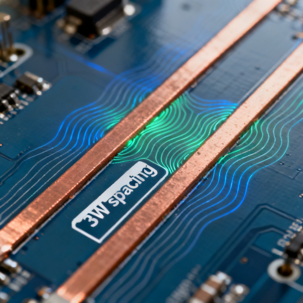
For decades, the 3W rule for crosstalk in high speed PCB design has been a golden guideline: to minimize crosstalk, the center-to-center spacing between two traces should be at least three times the width of a single trace. But at 56G PAM4 signaling, does this classic rule still provide sufficient isolation? This pillar content analyzes the physics, empirical data, and alternative spacing strategies for ultra-high-speed PCBs.
The Physics Behind the 3W Rule for Crosstalk in High Speed PCB
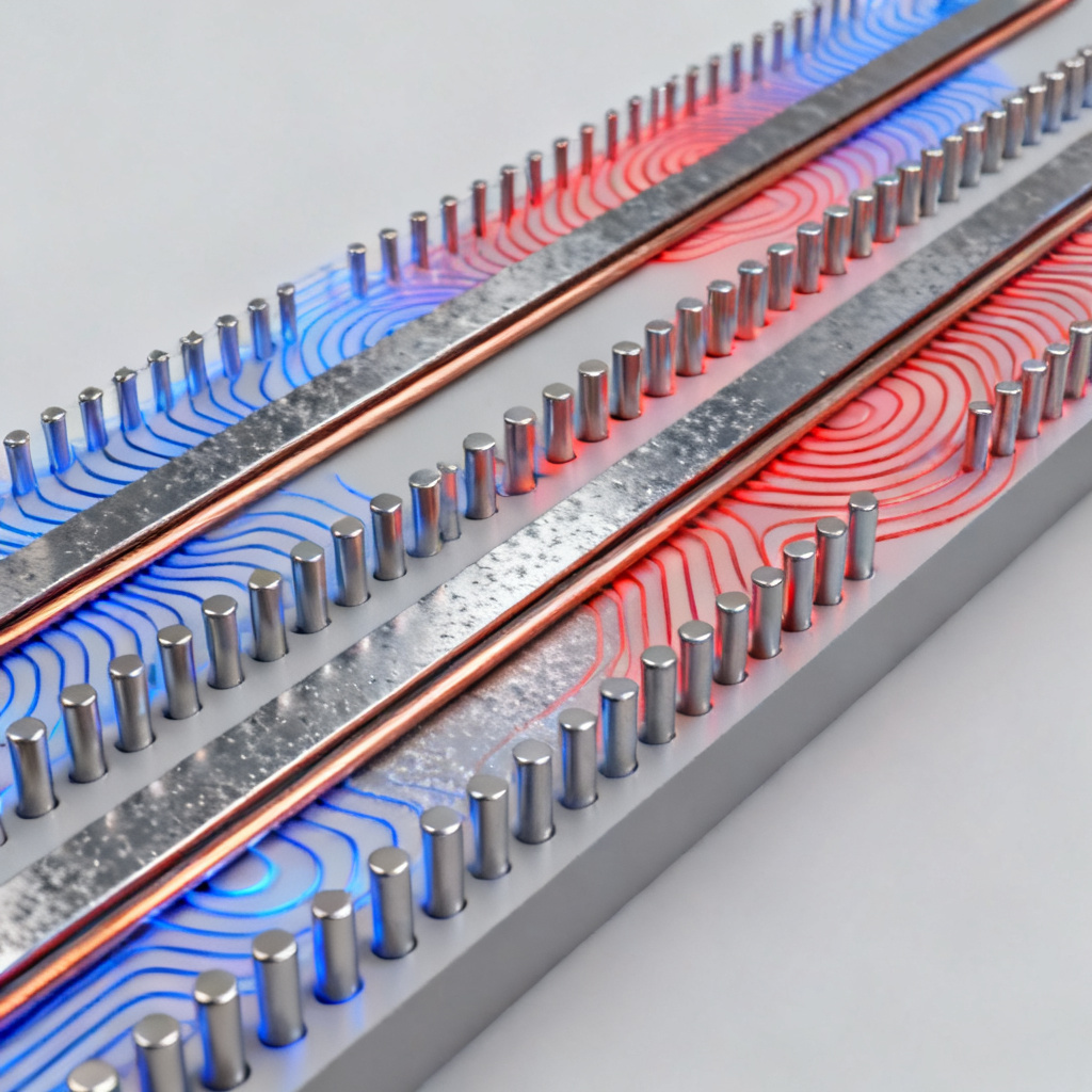
Before testing the rule, we must understand its foundation. The 3W rule for crosstalk in high speed PCB design was derived from a simple model of two microstrip lines on standard FR-4 substrate. Crosstalk arises from mutual capacitance (C_m) and mutual inductance (L_m) between adjacent traces. By placing the next trace’s edge at least 2 widths away (center-to-center = 3W), the mutual capacitance drops to <5% of the self-capacitance, and mutual inductance falls to <10% of self-inductance. This yields a near-end crosstalk (NEXT) coefficient of approximately -30 dB to -40 dB for typical digital signals—acceptable for most 1-5 Gbps designs.
Key Assumptions of the 3W Rule
This crosstalk rule implicitly assumes: trace width is the dominant geometric variable; rise time is much longer than propagation delay across the coupling length; and single-ended signaling is used. The rule was never intended for differential pairs, which have inherently lower crosstalk due to field cancellation. It works well for standard FR-4 with trace widths of 4-8 mils and signal rise times > 100 ps.
Why 56G PAM4 Changes Everything – The Failure of 3W
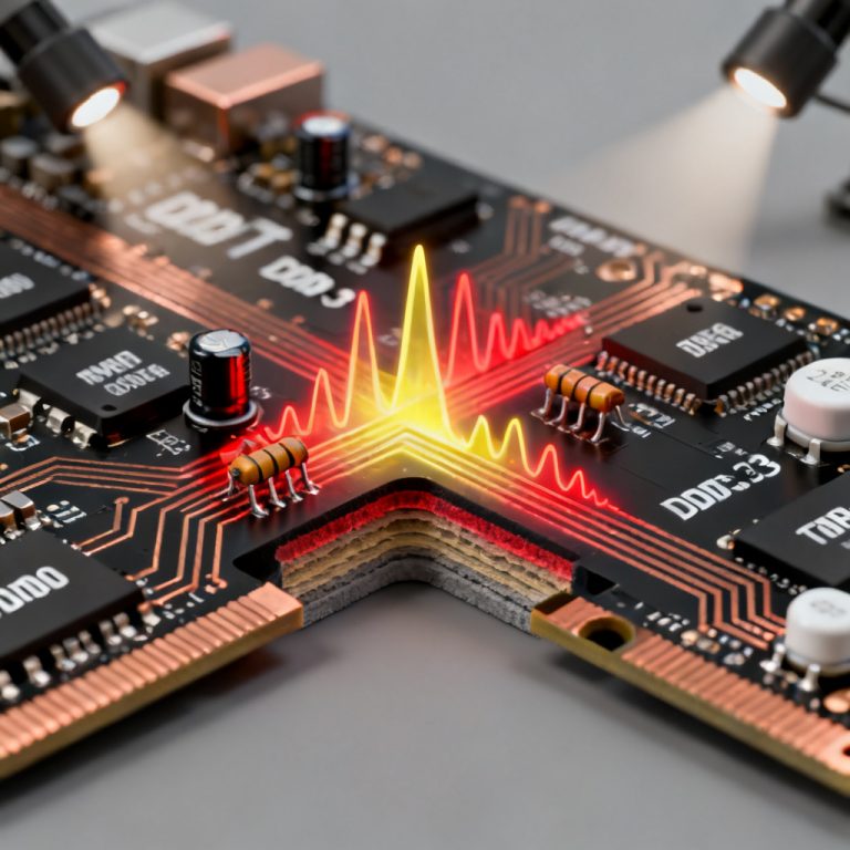
All authoritative sources converge on one critical point: the 3W rule for crosstalk in high speed PCB is insufficient for 56G PAM4. At 28 GBaud, the signal’s rise time shrinks to ~9 ps, making the line electrically long. Forward crosstalk (FEXT) becomes significant, and the 3W rule never addressed FEXT. Additionally, frequency-dependent dielectric loss and dispersion at 28 GHz cause increased attenuation and phase velocity mismatch, amplifying crosstalk.
The Impact of PAM4 Modulation
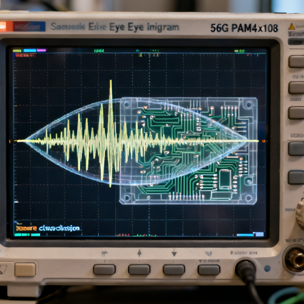
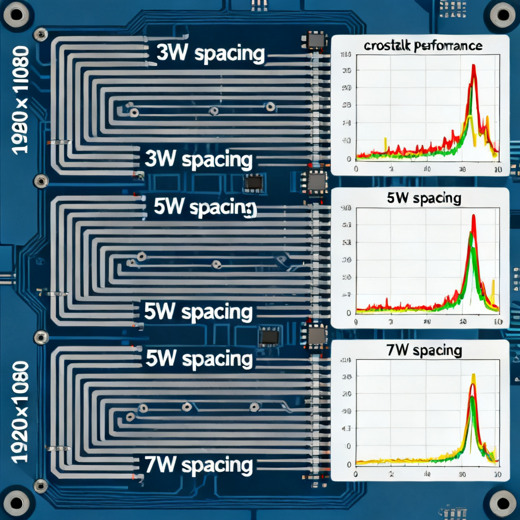
PAM4 uses four voltage levels with a smaller voltage swing, reducing signal-to-noise ratio by ~9.5 dB compared to NRZ. Crosstalk that was acceptable at -30 dB for NRZ becomes a direct bit-error-rate killer for PAM4. Empirical data shows that at 56G PAM4 with 5-mil traces and 15-mil spacing (3W), measured NEXT was -28 dB and FEXT was -22 dB at 12 inches length, causing a 40% eye height reduction—the link failed to meet IEEE 802.3bs mask margin requirements.
When Does the 3W Rule Still Work? – The Exceptions
Despite the failure at 56G, the 3W rule for crosstalk in high speed PCB remains useful in specific scenarios. For differential pairs, 3W spacing between pairs provides -40 dB NEXT up to 10 Gbps. In stripline geometry, the rule provides 6-10 dB better isolation than microstrip. For short traces under 2 inches, the coupling length is small enough that 3W spacing keeps NEXT below -40 dB even at 28 GHz.
Low-Speed Side Channels and Lossy Materials
On the same board, if a 56G channel is routed alongside a 1 Gbps control signal, the 3W rule is sufficient for the low-speed line. Counterintuitively, lossy materials like standard FR-4 can reduce FEXT because higher attenuation dampens the coupled wave, though this also degrades the primary signal.
What Spacing Does 56G Require? – The New Rules
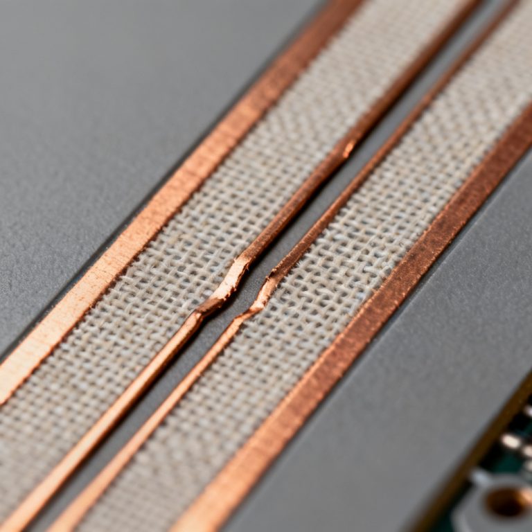
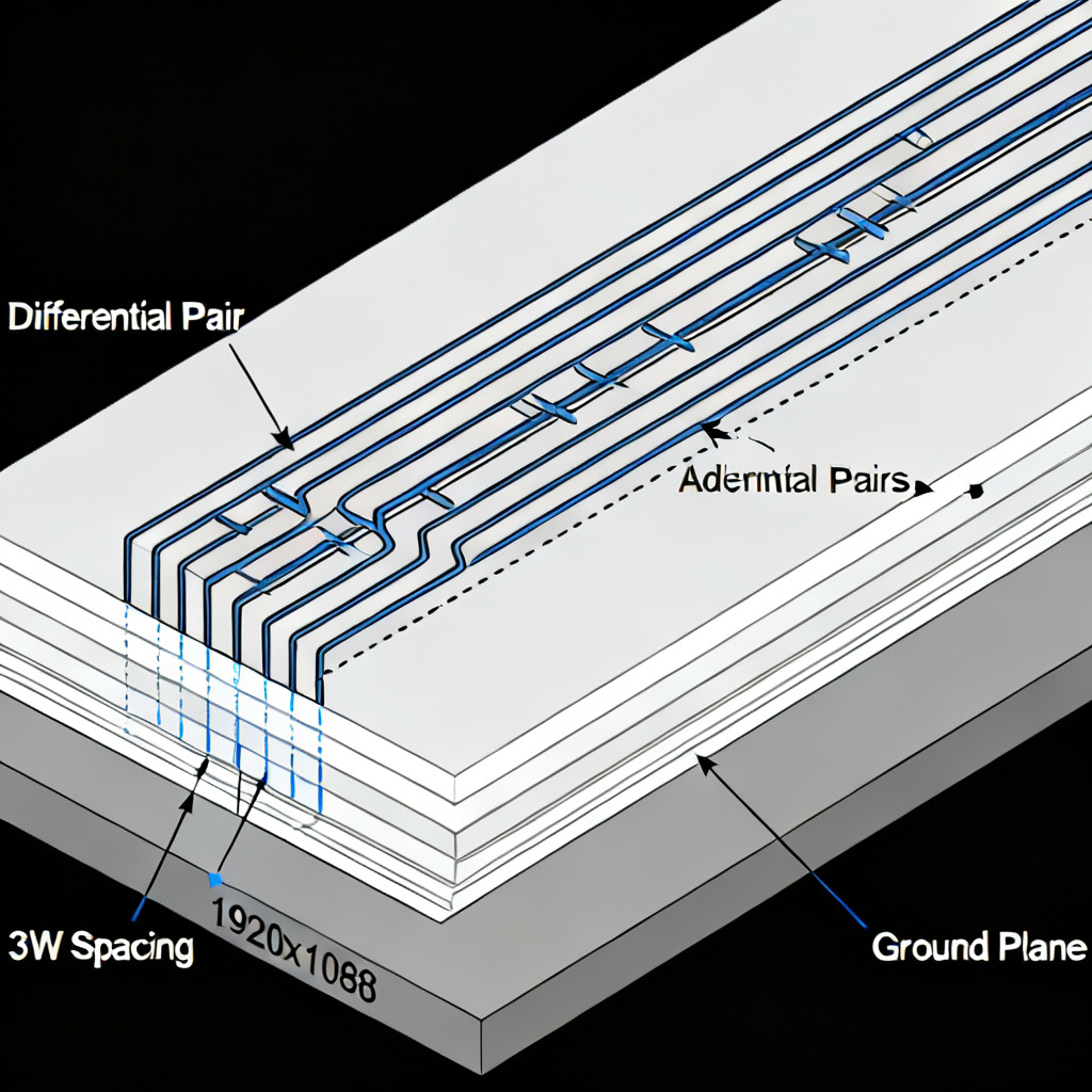
All sources propose alternatives: 5W to 7W spacing (center-to-center) for single-ended traces, or 3W for differential pair-to-pair spacing with additional shielding. For single-ended microstrip at 56G, use 5W spacing (e.g., 5-mil trace, 25-mil center-to-center, 20-mil gap) to achieve -40 dB NEXT and -35 dB FEXT for lengths up to 8 inches. For longer runs, use 7W spacing or switch to stripline.
Ground Via Fences and Guard Traces
Ground via fences are more effective than increasing spacing. Placing a row of ground vias (via pitch = λ/20 at 28 GHz, ~15 mils) between two traces reduces crosstalk by 15-20 dB. A guard trace grounded at both ends, placed at 2W from each signal trace, provides -50 dB isolation.
Practical Design Guidelines for Your 56G PCB
Synthesizing all sources, here is a step-by-step checklist for your next high-speed design:
| Parameter | Recommendation for 56G PAM4 |
|---|---|
| Stack-up | Use at least 12-layer board with dedicated ground planes; route all 56G signals on stripline layers |
| Spacing for single-ended | 5W center-to-center (4W gap); 7W if length > 8 inches |
| Spacing for differential pairs | 3W center-to-center between pairs (2W gap); add ground via fence if length > 6 inches |
| Shielding | Ground via fences at trace bundle edges; via spacing ≤ 15 mils |
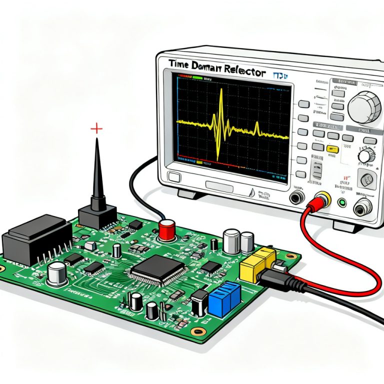
| Simulation | Use 3D full-wave EM simulation (e.g., Ansys HFSS, CST); target NEXT < -40 dB, FEXT < -35 dB |
| Material | Use low-loss materials like Megtron 6, Rogers 4350B, or Isola Tachyon 100G |
| Termination | Use AC-coupling capacitors with 0402 or 0201 package; avoid 90-degree bends |
| Maximum trace length | Keep under 12 inches; longer runs require redrivers or retimers |
By following these guidelines, you can ensure that your 3W rule for crosstalk in high speed PCB design is replaced with a robust, simulation-verified approach that meets 56G PAM4 performance requirements.
Frequently Asked Questions About the 3W Rule for Crosstalk in High Speed PCB
Does the 3W rule for crosstalk in high speed PCB work at 56G?
No, the 3W rule for crosstalk in high speed PCB fails at 56G PAM4 due to fast rise times, significant forward crosstalk, and lower SNR requirements. You need 5W to 7W spacing or ground via fences.
What spacing should I use instead of the 3W rule for crosstalk in high speed PCB at 56G?
For single-ended traces, use 5W center-to-center spacing. For differential pairs, use 3W spacing between pairs with ground via fences for lengths over 6 inches.
Can the 3W rule for crosstalk in high speed PCB still be used for differential pairs?
Yes, for differential pairs at 56G, 3W spacing between pairs provides adequate isolation for lengths under 6 inches, especially in stripline geometry.
What materials are best for 56G designs to complement the 3W rule for crosstalk in high speed PCB?
Low-loss materials like Megtron 6, Rogers 4350B, or Isola Tachyon 100G are recommended. Standard FR-4 is insufficient at 28 GHz.
How do ground via fences improve the 3W rule for crosstalk in high speed PCB?
Ground via fences reduce crosstalk by 15-20 dB, equivalent to increasing spacing from 3W to 10W, making them a space-efficient solution for dense boards.