Validating impedance control PCB results using VNA (S11/S22 measurement) is essential for high-speed designs where signal integrity is critical. This guide provides a complete, step-by-step methodology for engineers and QA teams to ensure your boards meet tight impedance tolerances.
Why VNA-Based Impedance Control PCB Validation Matters
In high-speed digital and RF PCB design, impedance control PCB validation is not optional—it is a fundamental requirement for signal integrity. A mismatch of even ±5% in characteristic impedance can cause reflections, ringing, and data errors at data rates above 1 Gbps. While TDR has been traditional, VNA-based S11/S22 measurements offer superior accuracy, frequency-domain insight, and repeatability for modern designs.
VNA vs. TDR for Impedance Control PCB Testing
A VNA measures scattering parameters in the frequency domain. For impedance control PCB validation, S11 (input reflection coefficient) and S22 (output reflection coefficient) are critical. VNA provides higher accuracy at high frequencies and better repeatability than TDR, making it the preferred method for production validation.
| Parameter | TDR | VNA (S11/S22) |
|---|---|---|
| Domain | Time domain | Frequency domain |
| Resolution | Limited by rise time | Extremely high |
| Accuracy at high frequencies | Degrades | Maintains accuracy |
| Repeatability | Moderate | Excellent |
Preparing for Impedance Control PCB Measurement
Design for Testability Requirements
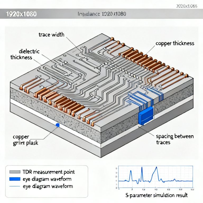
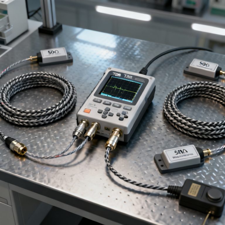
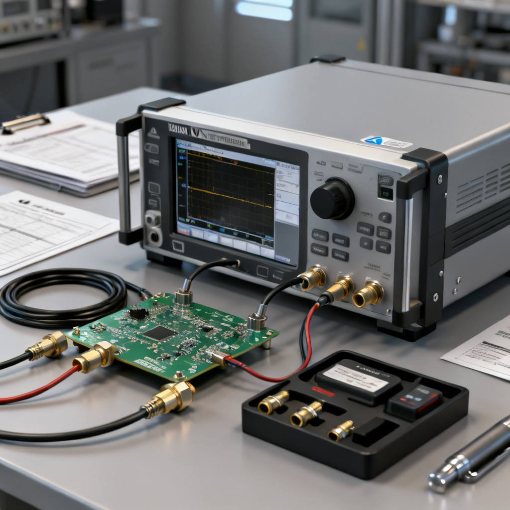
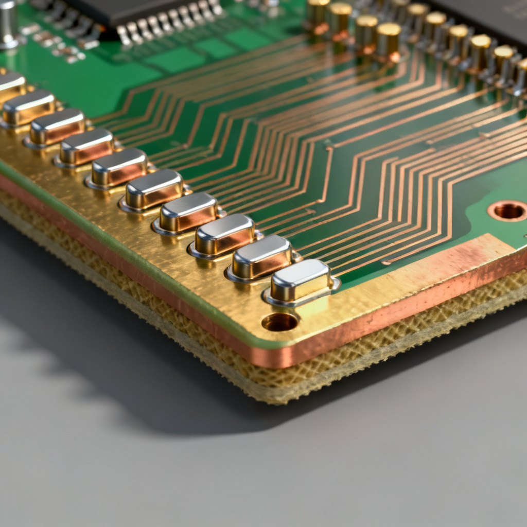
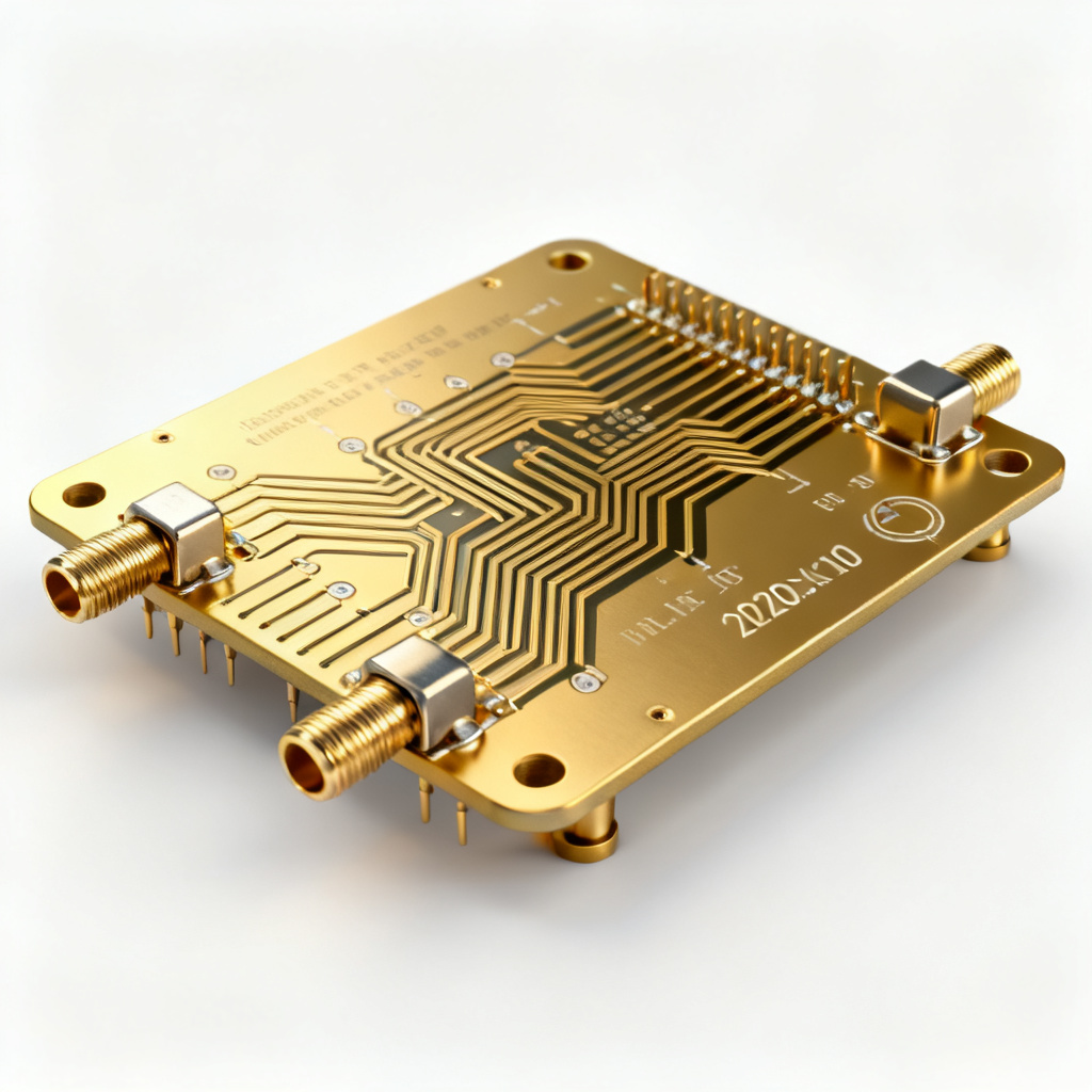
Before any impedance control PCB measurement, your board must include proper test structures. Impedance coupons should be at least 3 inches long, terminated with a precision 50 Ω load, and placed on the same layer as the trace being validated. Launch structures using SMA connectors or RF probes ensure reliable VNA connections.
Calibration for Accurate Impedance Control PCB Results
VNA calibration removes systematic errors. For impedance control PCB validation, use SOLT (Short-Open-Load-Through) for coaxial measurements or TRL for on-wafer probing. Always calibrate at the same temperature as measurements—a 10°C change can shift impedance by 0.5–1 Ω.
De-Embedding Fixture Effects
If test fixtures are used, their parasitics will corrupt impedance control PCB results. Use the 2x-Thru method, automated fixture removal, or time gating to isolate the DUT reflection from connector reflections.
Step-by-Step VNA Measurement Procedure for Impedance Control PCB
Step 1: Configure the VNA
Set frequency range from 10 MHz to at least 5× the highest operating frequency. Use 201+ points, 1 kHz IF bandwidth, and -10 dBm power level for impedance control PCB testing.
Step 2: Connect the DUT
Use a torque wrench for consistent connector mating. For single-ended traces, connect Port 1 to the trace input. For differential traces, use a balun or 4-port VNA to measure Sdd11.
Step 3: Perform Calibration
Choose SOLT calibration. Connect standards in order: Open → Short → Load → Thru. Verify calibration by measuring a known 50 Ω load—S11 should be below -40 dB.
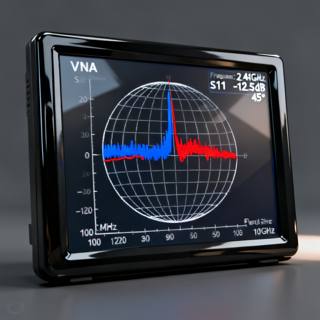
Step 4: Measure S11 and Convert to Impedance
Record S11 magnitude and phase. Convert to impedance using: Zin = 50 × (1 + S11) / (1 – S11). Plot impedance vs. frequency; a well-designed impedance control PCB should show flat impedance within ±2 Ω of target.
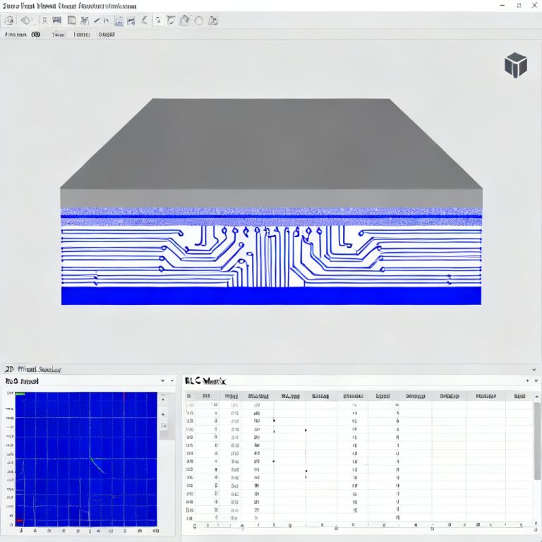
Step 5: Validate with Time-Domain Transform
Modern VNAs can perform an inverse Fourier transform to display impedance vs. distance. Apply a window function, set time range to cover trace length, and read impedance at the midpoint—this combines frequency-domain accuracy with time-domain visualization.
Interpreting Impedance Control PCB Results
Acceptable Impedance Tolerances
| Target Impedance | Standard Tolerance | High-Reliability Tolerance |
|---|---|---|
| 50 Ω (single-ended) | ±10% (45–55 Ω) | ±5% (47.5–52.5 Ω) |
| 100 Ω (differential) | ±10% (90–110 Ω) | ±5% (95–105 Ω) |
| 75 Ω (video) | ±10% (67.5–82.5 Ω) | ±5% (71.25–78.75 Ω) |
S11 Limits for Impedance Control PCB Validation
For digital designs up to 5 Gbps, S11 should be below -15 dB; for 5–25 Gbps, below -20 dB; for RF/microwave up to 20 GHz, below -25 dB; and for millimeter-wave above 30 GHz, below -30 dB.
Common Failure Modes
If impedance control PCB results show impedance too high, trace width may be too narrow or dielectric thickness too large. If too low, trace width may be too wide or etch undercut present. Impedance ripple vs. frequency indicates resonances from stub lengths or connector discontinuities.
Advanced Impedance Control PCB Validation Techniques
Differential Impedance Validation
For differential pairs, measure Sdd11 and convert to differential impedance using: Zdiff = 2 × Z0 × (1 + Sdd11) / (1 – Sdd11). For a 100 Ω target, Sdd11 should be below -20 dB.
Mixed-Mode S-Parameters
Convert standard S-parameters to mixed-mode for coupled lines. High Scd11 indicates poor symmetry—a common issue in impedance control PCB fabrication.
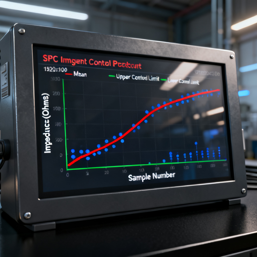
Statistical Process Control for Production
Use VNA measurements to build control charts. Measure impedance on 5–10 coupons per panel, calculate mean and standard deviation, set control limits at ±3σ, and flag panels exceeding ±5% of target.
Best Practices for Impedance Control PCB Validation
Do’s
Use a calibrated reference plane, measure at multiple frequencies, document conditions, use averaging, and validate with a known good board.
Don’ts
Don’t use uncalibrated cables, ignore connector effects, measure on a powered board, assume TDR and VNA give identical results, or use low-quality test coupons.
Choosing the Right VNA for Impedance Control PCB Testing
| VNA Type | Frequency Range | Use Case |
|---|---|---|
| Benchtop (High-End) | 10 MHz – 67 GHz | R&D, RF/microwave design |
| Benchtop (Mid-Range) | 9 kHz – 26.5 GHz | High-speed digital, production QA |
| Portable/Field | 1 MHz – 20 GHz | On-site validation |
| USB/Compact | 1 MHz – 8.5 GHz | Low-cost production testing |
Case Study: Validating a 50 Ω Microstrip Impedance Control PCB
A customer required 50 Ω ±5% on a 10-layer board with Isola 370HR dielectric. Using a Keysight E5080B with SOLT calibration, S11 at 10 GHz was -28.3 dB, impedance was 49.2 Ω, and ripple was ±0.8 Ω across 1–20 GHz. The board passed validation and production was approved.
Frequently Asked Questions About Impedance Control PCB Validation
Can I use a VNA to measure impedance on a populated board?
No. VNA measurements require a passive DUT. Active components will distort reflections and can damage the VNA.
What is the difference between S11 and return loss?
Return loss is the negative of S11 in dB. Both indicate reflection magnitude for impedance control PCB validation.
How often should I recalibrate the VNA?
At minimum once per day. Recalibrate if cables are moved or temperature changes by more than 5°C.
What is the minimum trace length for VNA impedance validation?
At least 3 inches for frequencies below 10 GHz. Shorter traces suffer from launch parasitics.
Does VNA impedance validation replace TDR?
No. TDR is better for detecting localized defects; VNA is better for overall accuracy. Use both for comprehensive impedance control PCB validation.
At [Your Company Name], we integrate VNA validation into every high-speed PCB production run. Contact us to discuss your impedance control PCB requirements or request a free validation report.