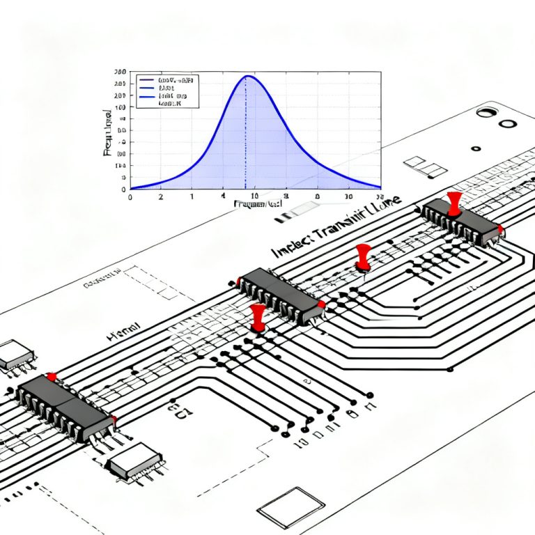
In high-speed PCB design, trace spacing directly affects crosstalk—unwanted electromagnetic coupling between adjacent traces. This pillar content on how trace spacing affects crosstalk in high speed PCB consolidates expert knowledge from Altium, Sierra Circuits, and Cadence to provide you with complete equations and rules of thumb for reliable signal integrity.
How Trace Spacing Affects Crosstalk in High Speed PCB: Key Mechanisms
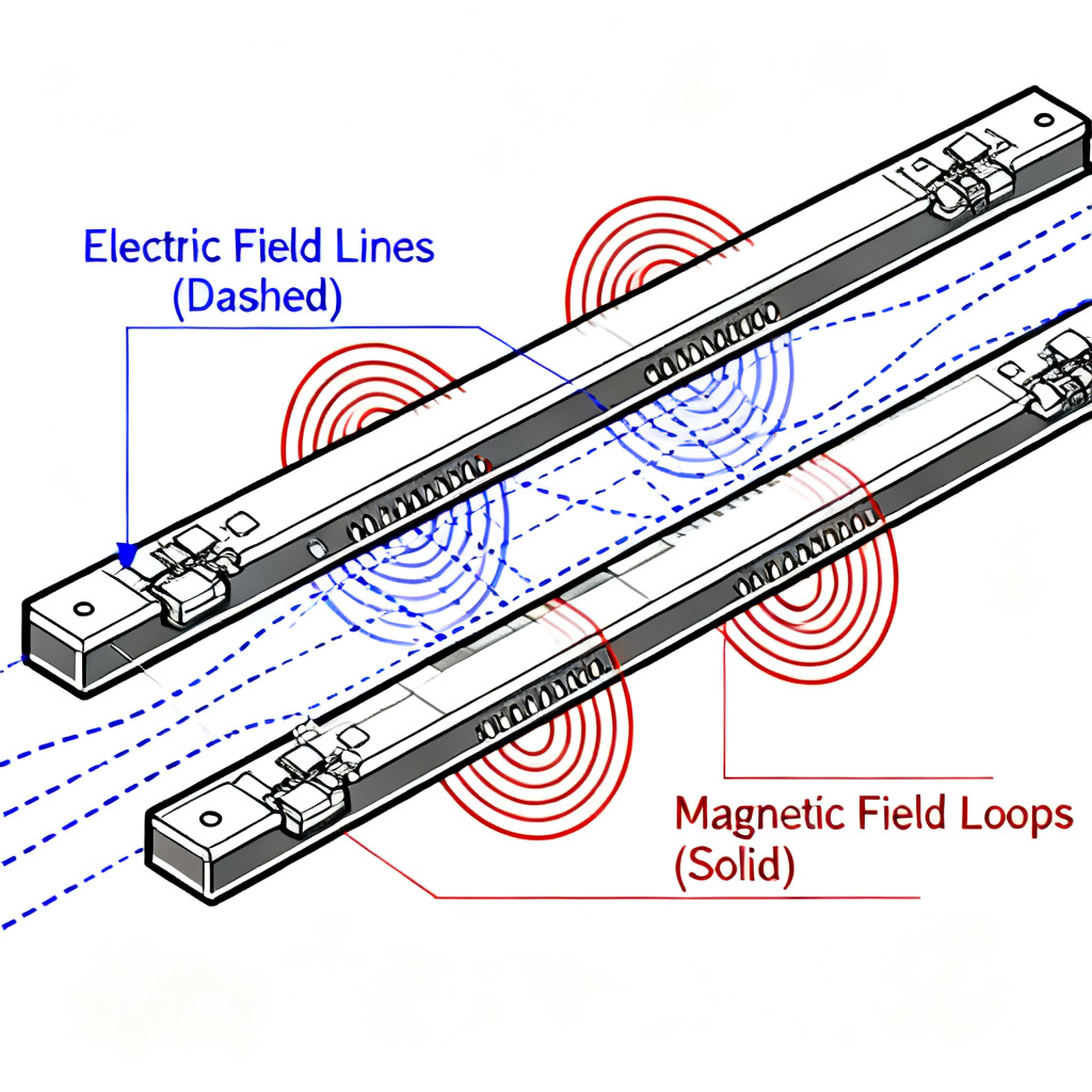
Crosstalk arises from two primary coupling mechanisms: capacitive (electric field) and inductive (magnetic field) coupling. In high-speed PCB design, both become significant due to fast edge rates (dV/dt and dI/dt).
Capacitive Coupling and Trace Spacing
Capacitive coupling occurs when the electric field from a trace (aggressor) induces a voltage on a neighboring trace (victim). The mutual capacitance (Cm) between traces is inversely proportional to their spacing (S). As spacing decreases, Cm increases, leading to higher crosstalk.
Key Equation (from Altium): The near-end crosstalk (NEXT) coefficient for capacitive coupling in a microstrip line is approximated by: K_NEXT,cap = 1/4 * (Cm / (C11 + Cm)). Where Cm = mutual capacitance per unit length, C11 = self-capacitance of the trace to ground.
Inductive Coupling and Trace Spacing
Inductive coupling results from the magnetic field of the aggressor trace inducing a current in the victim trace. The mutual inductance (Lm) decreases as spacing increases.
Key Equation (from Sierra Circuits): For microstrip lines, the inductive coupling coefficient (Kb) is: Kb = Lm / L11. Where Lm = mutual inductance, L11 = self-inductance of the trace.
Total Crosstalk in High Speed PCB
The total crosstalk at the near end (NEXT) and far end (FEXT) combines both capacitive and inductive contributions. For homogeneous dielectric microstrip lines, NEXT is dominant, while FEXT can be significant in stripline configurations.
From Cadence: The total NEXT voltage (V_next) is given by: V_next = 1/4 * (Cm/C11 + Lm/L11) * V_aggressor. For microstrip, the inductive component often dominates, making spacing critical.
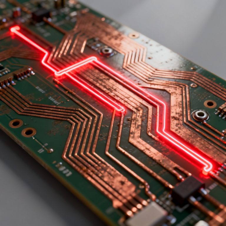
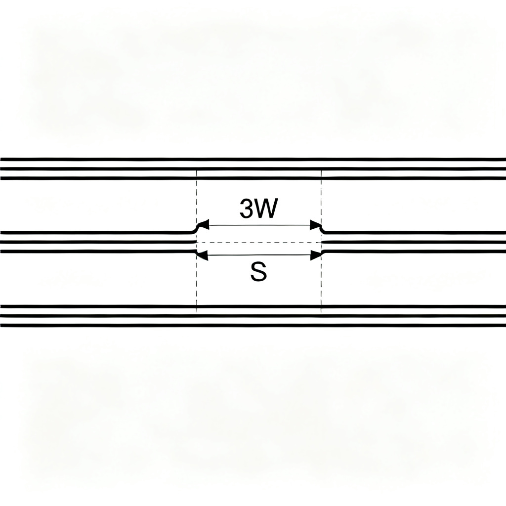
The 3W Rule: A Classic Rule of Thumb for Trace Spacing
Before applying rules of thumb, let’s examine how trace spacing affects crosstalk in high speed PCB mathematically. The most widely cited rule of thumb for trace spacing is the 3W Rule, where the center-to-center spacing between traces is at least three times the trace width (W). This is a foundational concept in high-speed PCB design.
What the 3W Rule Achieves
From Altium: The 3W rule reduces crosstalk to approximately 1-2% of the aggressor signal amplitude. This is sufficient for many low-to-moderate speed designs (e.g., < 1 Gbps). From Sierra Circuits: At 3W spacing, the mutual coupling drops by about 90% compared to minimum spacing (1W). However, this rule is a rough guideline and may fail for high-speed signals (e.g., > 5 Gbps) or long parallel runs.
Limitations of the 3W Rule
From Cadence: The 3W rule does not account for dielectric stack-up, trace length, or signal rise time. For high-speed designs (e.g., DDR4, PCIe Gen 4), 5W or even 10W spacing may be required. From all sources: The rule assumes a homogeneous medium and does not differentiate between microstrip and stripline. In stripline, coupling is lower due to ground plane shielding, so 2W may suffice.
Practical Application of the 3W Rule
When to use 3W: For clock lines, parallel data buses, or analog signals in mixed-signal designs. When to exceed 3W: For differential pairs, high-speed serial links (e.g., USB 3.0, HDMI), or when rise time is < 100 ps.
Key Equations for Calculating Crosstalk vs. Trace Spacing
To move beyond rules of thumb, engineers use analytical equations. Here are the most critical ones from the three sources for high-speed PCB design.
Mutual Capacitance and Inductance Formulas
From Altium (for microstrip lines): The mutual capacitance per unit length (Cm) is: Cm = (ε0 εr / π) * ln(1 + 2h/S), where h = dielectric height, S = edge-to-edge spacing. The mutual inductance per unit length (Lm) is: Lm = (μ0 / 2π) * ln(1 + 2h/S).
From Sierra Circuits (for stripline): For stripline, the equations are more complex due to top and bottom ground planes: Cm ≈ (ε0 εr / π) * ln((S + w)/S), where w = trace width.
Crosstalk Coefficient (K) as a Function of Spacing
From Cadence: The near-end crosstalk coefficient (K_NEXT) for a microstrip line is approximated by: K_NEXT ≈ 1/4 * (1 / (1 + 2h/S)). This shows that doubling spacing from 1W to 2W reduces K_NEXT by roughly 50%.
Saturation Length and Spacing
From all sources: Crosstalk saturates after a certain parallel trace length (L_sat). For microstrip: L_sat = tr / (2 * vp), where tr = rise time, vp = propagation velocity (approx. 6 in/ns for FR4). If the parallel length exceeds L_sat, further spacing increases have diminishing returns. For a 1 ns rise time, L_sat is about 3 inches.
Practical Design Rules of Thumb for High Speed PCB
Based on the three expert sources, here are actionable rules for your high-speed PCB designs.
General Spacing Guidelines
- Minimum spacing: 2W for low-speed or short traces (< 1 inch).
- Recommended spacing: 3W for moderate-speed signals (1-5 Gbps).
- High-speed spacing: 5W or more for signals > 5 Gbps or rise times < 200 ps.
From Altium: For differential pairs, maintain 2W spacing within the pair and 5W to adjacent traces.
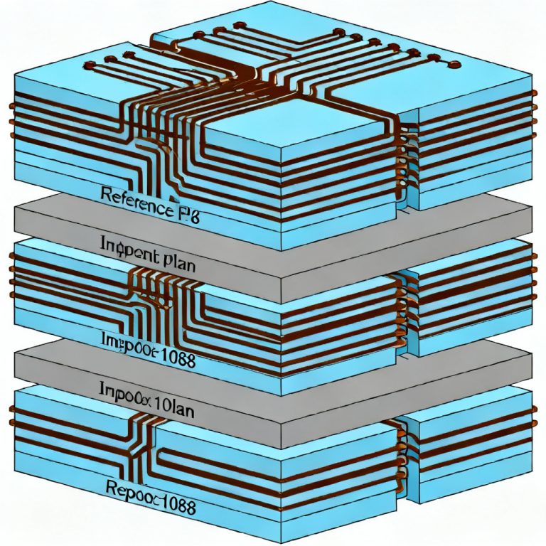
Layer Stack-Up Considerations
Microstrip vs. Stripline: Stripline has ~50% less crosstalk than microstrip for the same spacing due to ground plane shielding. Use stripline for critical high-speed nets. From Sierra Circuits: In microstrip, increase spacing by 20-30% if the dielectric height (h) is small (< 4 mils).
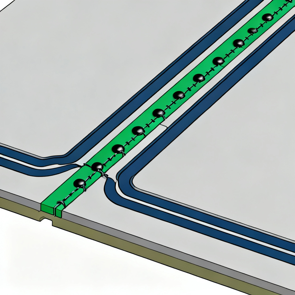
Guard Traces and Grounding
From Cadence: Adding a grounded guard trace between aggressor and victim can reduce crosstalk by 10-15 dB, but only if the guard trace is stitched to ground with vias at intervals < λ/20 (e.g., every 100 mils for 10 GHz). From Altium: Guard traces are less effective at high frequencies (> 1 GHz) due to resonance. Instead, increase spacing.
Length Matching and Timing
From all sources: For parallel buses (e.g., DDR), ensure trace lengths are matched within 10% of the rise time distance to minimize skew-induced crosstalk.
Advanced Considerations for High Speed PCB Design
These advanced topics are critical for engineers pushing the boundaries of high-speed PCB design.
Frequency-Dependent Effects
From Sierra Circuits: At frequencies > 1 GHz, skin effect and dielectric losses increase, altering the crosstalk profile. Spacing must be recalculated using 3D field solvers (e.g., Ansys HFSS or CST). From Cadence: The crosstalk coefficient becomes frequency-dependent. For example, at 10 GHz, a 3W spacing may only reduce crosstalk to 5% instead of 1%.
Differential Pair Spacing
From Altium: For differential pairs (e.g., LVDS, USB), intra-pair spacing determines impedance (typically 5-10 mils for 100Ω). Inter-pair spacing should be at least 3x the intra-pair spacing to minimize common-mode crosstalk. From all sources: Keep differential pairs tightly coupled (small intra-pair spacing) to reduce radiated emissions and susceptibility.
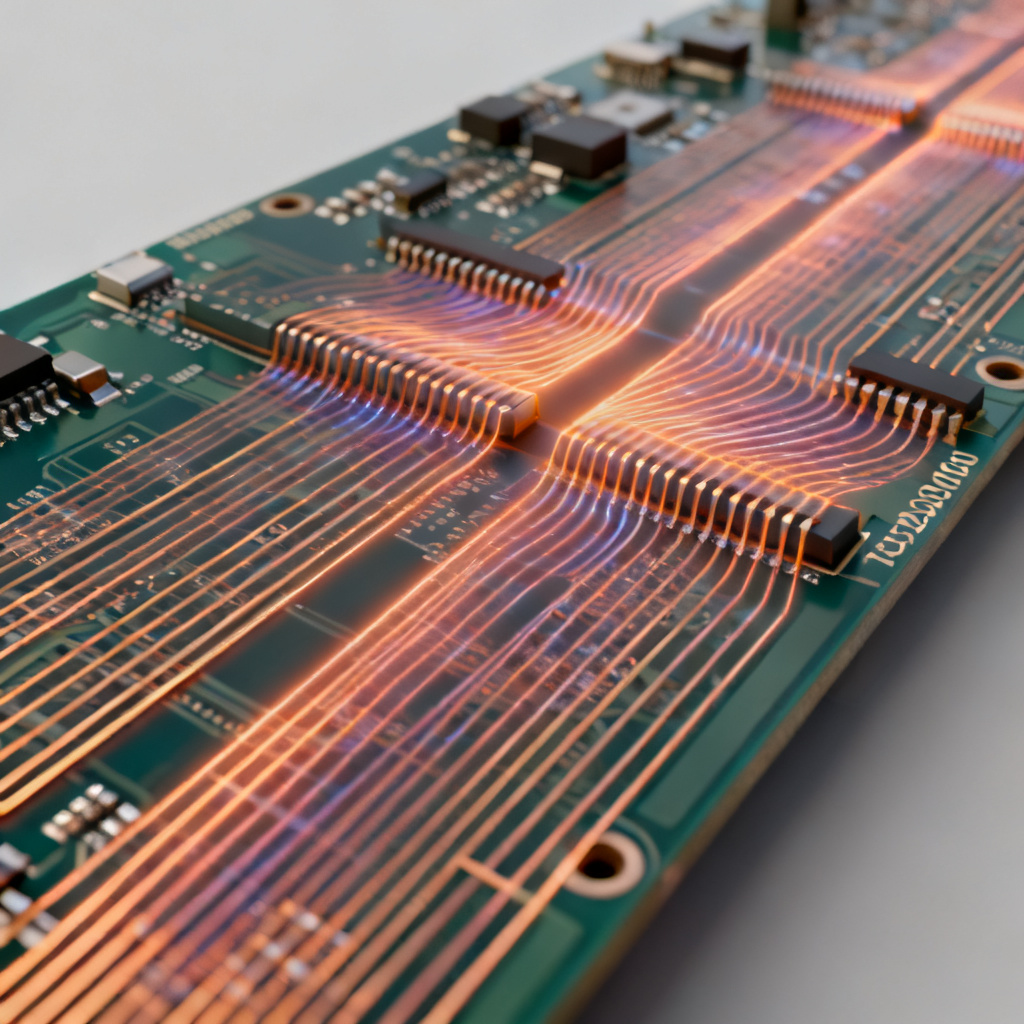
Via Stubs and Crosstalk
From Cadence: Via stubs can act as antennas, coupling crosstalk between layers. Use back-drilling or blind vias for high-speed signals to minimize stub length.
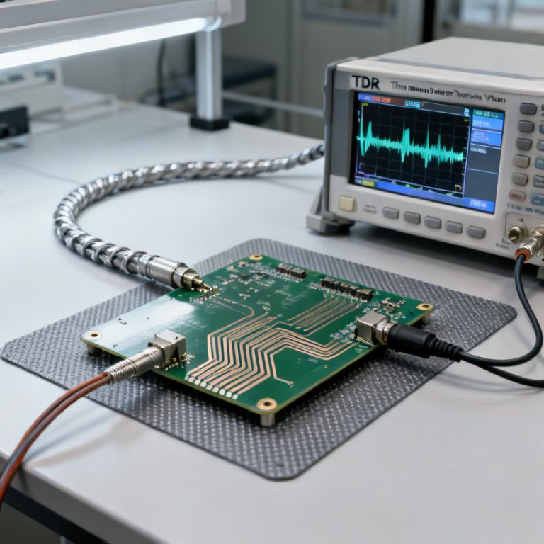
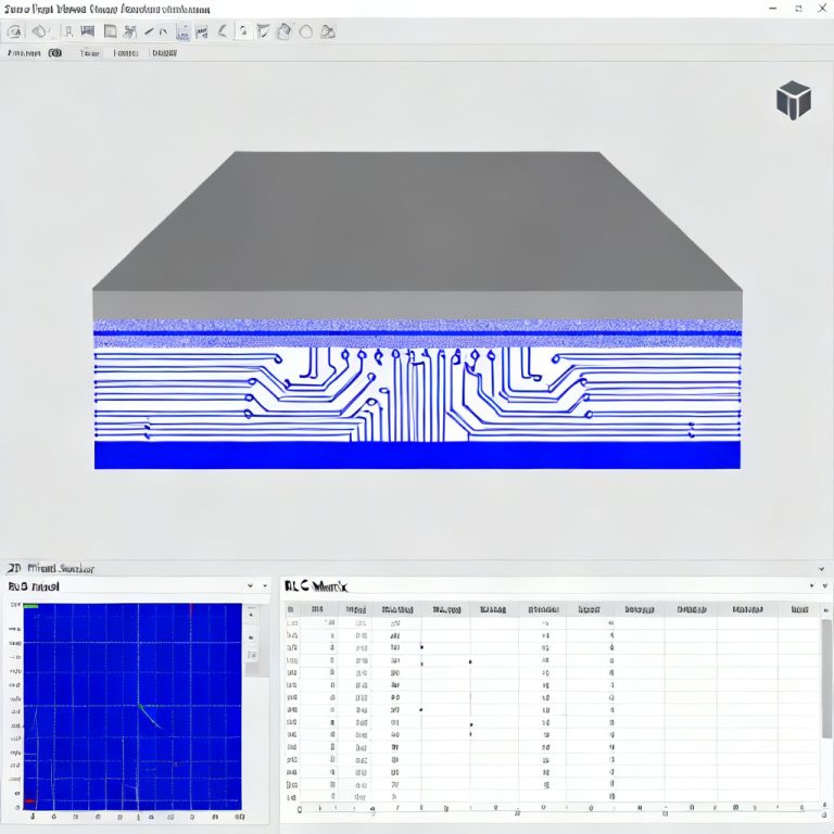
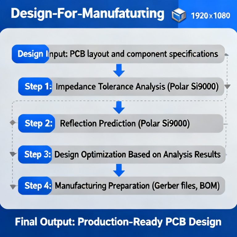
Simulation and Verification for Trace Spacing
Simulation is essential for validating trace spacing in high-speed PCB design.
When to Simulate
From all sources: Always simulate for designs with rise times < 500 ps, parallel trace lengths > 2 inches, or data rates > 5 Gbps. Use tools like HyperLynx, ADS, or Sigrity.
Key Simulation Parameters
From Altium: Set up a 3D model with your stack-up, trace geometry, and material properties (Dk, Df). Run a time-domain reflectometry (TDR) simulation to measure crosstalk. From Sierra Circuits: Use a coupled transmission line model to extract S-parameters. Look at S31 (near-end crosstalk) and S41 (far-end crosstalk).
Acceptance Criteria
From Cadence: For most high-speed designs, keep NEXT < -30 dB and FEXT < -35 dB. For sensitive analog or clock signals, target < -40 dB.
Case Studies and Examples for High Speed PCB
Real-world applications demonstrate how trace spacing rules apply in high-speed PCB design.
Example 1: DDR4 Memory Bus
- Requirement: 3200 MT/s, rise time 200 ps.
- Spacing rule: Use 5W for address/command lines, 3W for data lines (with length matching).
- Result: Crosstalk reduced to < 2% per the Sierra Circuits guideline.
Example 2: PCIe Gen 4 Differential Pair
- Requirement: 16 GT/s, intra-pair spacing 8 mils (for 100Ω).
- Spacing rule: Inter-pair spacing = 25 mils (3x intra-pair).
- Result: NEXT < -35 dB per Cadence simulation.
Example 3: 10 Gbps Ethernet (XFI)
- Requirement: Single-ended microstrip, rise time 50 ps.
- Spacing rule: Use 10W spacing (e.g., 50 mils for 5 mil trace width) with grounded coplanar waveguide (GCPW) structure.
- Result: Crosstalk < -40 dB per Altium analysis.
Common Mistakes in High Speed PCB Trace Spacing
Avoid these pitfalls to ensure reliable high-speed PCB design.
- Ignoring Rise Time: Relying solely on the 3W rule without considering rise time can lead to failures. Always calculate L_sat.
- Overlooking Ground Plane Integrity: Poor ground plane continuity (e.g., slots) increases inductive coupling.
- Using Guard Traces Incorrectly: Ungrounded guard traces act as resonators, worsening crosstalk.
- Neglecting Layer Transitions: Vias between layers can introduce crosstalk if not properly shielded.
Conclusion: Best Practices for High Speed PCB Trace Spacing
Trace spacing is the most effective and cost-efficient method to control crosstalk in high-speed PCB design. By combining the 3W rule with analytical equations and simulation, you can achieve reliable signal integrity.
Final Recommendations from the Experts:
- Start with 3W for moderate-speed designs.
- Scale to 5W or more for high-speed signals (> 5 Gbps).
- Use stripline for critical nets.
- Simulate when in doubt.
- Partner with a trusted PCB manufacturer like [Your Company Name] to ensure stack-up and material choices align with your spacing requirements.
Frequently Asked Questions About Trace Spacing in High Speed PCB
What is the 3W rule in high-speed PCB design?
The 3W rule states that trace spacing should be at least three times the trace width to reduce crosstalk to acceptable levels in high-speed PCB design.
How does trace spacing affect crosstalk in high-speed PCBs?
Trace spacing directly impacts mutual capacitance and inductance between traces; larger spacing reduces crosstalk by weakening electromagnetic coupling in high-speed PCB design.
What is the minimum trace spacing for 10 Gbps signals?
For 10 Gbps signals, a minimum of 5W to 10W spacing is recommended, depending on rise time and stack-up, to maintain signal integrity in high-speed PCB design.
Can guard traces replace increased trace spacing?
Guard traces can reduce crosstalk by 10-15 dB but are less effective above 1 GHz; increasing trace spacing is generally more reliable in high-speed PCB design.
What is the difference between NEXT and FEXT in PCB crosstalk?
Near-end crosstalk (NEXT) occurs at the aggressor’s input, while far-end crosstalk (FEXT) occurs at the victim’s output; both are influenced by trace spacing in high-speed PCB design.
Why Choose Our High Speed PCB Manufacturing Services
Our high-speed PCB manufacturing services ensure precise trace spacing control, advanced stack-up design, and rigorous simulation to minimize crosstalk. We offer competitive lead times and expert engineering support.
| Signal Type | Recommended Trace Spacing | Maximum Crosstalk Reduction |
|---|---|---|
| Low-speed (< 1 Gbps) | 2W | ~70% |
| Moderate-speed (1-5 Gbps) | 3W | ~90% |
| High-speed (> 5 Gbps) | 5W to 10W | >95% |