Master the Lattice Diagram Method for transmission line reflections in high-speed PCB design. This step-by-step guide with bounce diagrams, impedance mismatches, and termination optimization helps you visualize wave propagation and ensure signal integrity in your custom high-speed PCB projects.

1. Fundamentals of Lattice Diagram Method for Transmission Line Reflections
The Lattice Diagram Method is a graphical tool that visualizes voltage and current wave propagation along a transmission line. Understanding reflections is critical for high-speed PCB design, where impedance mismatches cause signal degradation.
1.1 Voltage and Current Waves in Lattice Diagram Method
In any transmission line, instantaneous voltage equals the sum of forward-traveling wave (V⁺) and backward-traveling wave (V⁻). Current follows I = (V⁺ – V⁻) / Z₀. The Lattice Diagram Method tracks these waves at each time step.
1.2 Reflection Coefficients for Lattice Diagram Method
Reflection coefficients at source (Γₛ) and load (Γₗ) determine wave behavior: Γ = (Z – Z₀) / (Z + Z₀). Key values: open circuit Γ=+1, short circuit Γ=-1, matched Γ=0. The Lattice Diagram Method uses these coefficients to calculate reflected waves.
1.3 Time of Flight in Lattice Diagram Method
The one-way propagation delay (TD = length / velocity) defines the time grid. Each diagonal line in the Lattice Diagram Method represents a wave traveling between source and load.
2. Step-by-Step Construction of a Lattice Diagram for High-Speed PCB
This section provides a systematic procedure for building a Lattice Diagram Method for your high-speed PCB designs.
2.1 Define System Parameters for Lattice Diagram Method
Record Z₀, Zₛ, Zₗ, Γₛ, Γₗ, source voltage Vₛ, and TD. These inputs drive the entire Lattice Diagram Method calculation.
2.2 Calculate Initial Incident Wave V₁⁺
Use voltage divider: V₁⁺ = Vₛ × [Z₀ / (Zₛ + Z₀)]. This wave launches from source at t=0 in the Lattice Diagram Method.
2.3 Draw the Lattice Grid
Create a time-position grid with diagonal lines. Each forward diagonal represents a wave traveling from source to load; each backward diagonal represents a reflected wave. The Lattice Diagram Method visualizes this clearly.
2.4 Trace Reflections and Calculate Voltages
At each boundary, multiply incident wave by reflection coefficient to get reflected wave. Sum all waves at each time step to find transient voltage. The Lattice Diagram Method iterates this process until reflections become negligible.
2.5 Plot Transient Response
Using calculated voltages at load and source, plot time-domain waveform. This output from the Lattice Diagram Method guides termination decisions for your high-speed PCB.
3. Practical Examples of Lattice Diagram Method for PCB Engineers
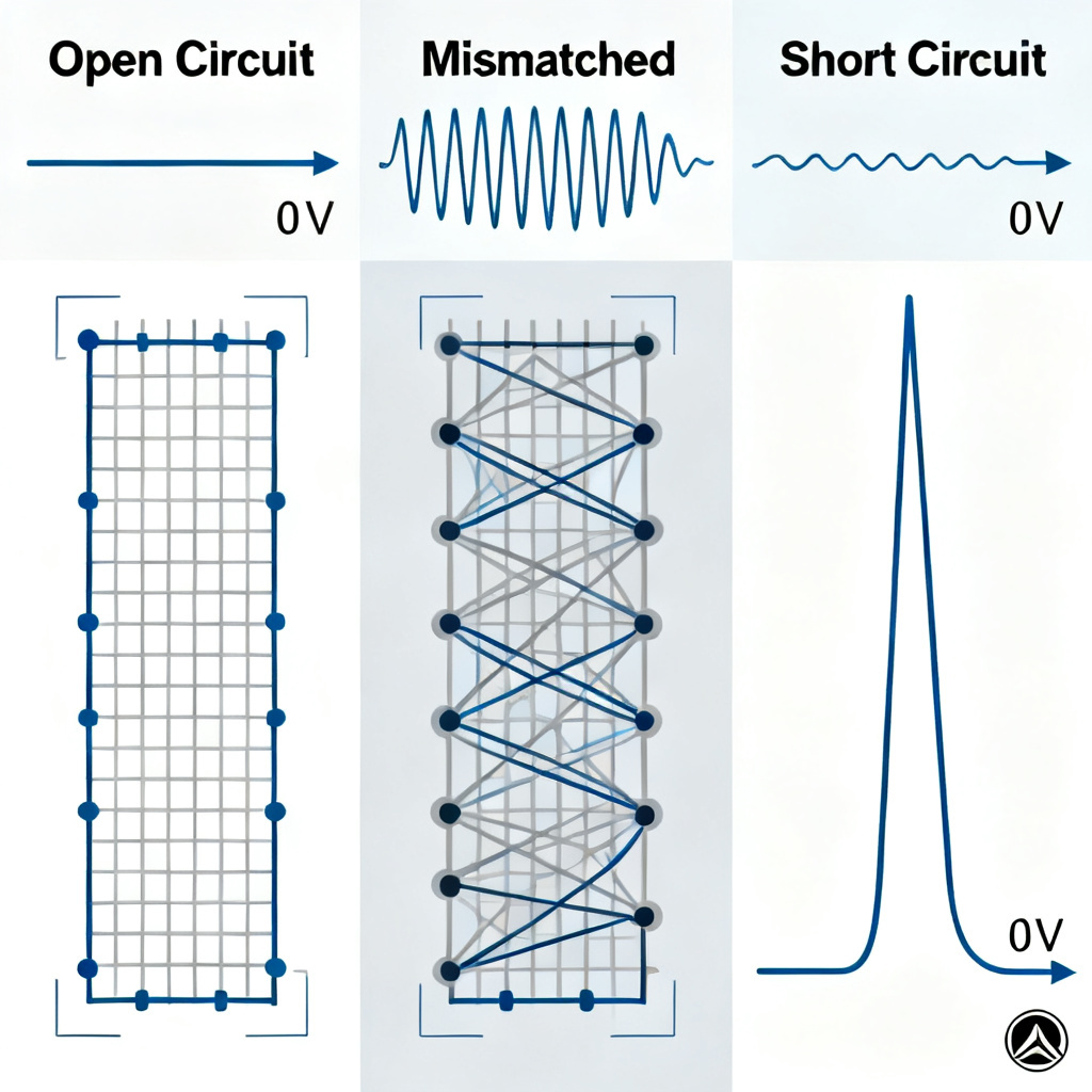
3.1 Open Circuit Load Example
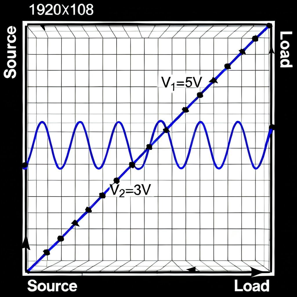
Parameters: Zₛ=50Ω, Z₀=50Ω, Zₗ=∞, Vₛ=2V. Γₛ=0, Γₗ=+1. V₁⁺=1V. At t=TD, load voltage = 2V. At t=2TD, source voltage = 2V. The Lattice Diagram Method shows immediate steady state due to matched source.
3.2 Both Source and Load Reflective Example
Parameters: Zₛ=25Ω, Z₀=50Ω, Zₗ=100Ω, Vₛ=3V. Γₛ=-0.333, Γₗ=+0.333. V₁⁺=2V. Multiple reflections approach steady state of 2.4V. The Lattice Diagram Method reveals each bounce contribution for impedance control.
3.3 Short Circuit Load Example
Parameters: Zₛ=50Ω, Z₀=50Ω, Zₗ=0, Vₛ=1V. Γₛ=0, Γₗ=-1. V₁⁺=0.5V. Load voltage reaches 0V at t=TD. The Lattice Diagram Method confirms zero steady state.
4. Advanced Applications of Lattice Diagram Method in High-Speed PCB Design
4.1 Termination Strategy Optimization
Use the Lattice Diagram Method to simulate series, parallel, or AC terminations before prototyping. Series termination (Rₛ + Z₀ = Zₛ) absorbs reflections at source, eliminating multiple bounces in your custom high-speed PCB.
4.2 Clock and Data Bus Design
In multi-drop buses (e.g., DDR memory), reflections from unmatched stubs cause signal eye closure. The Lattice Diagram Method predicts worst-case overshoot and undershoot, guiding stub length and termination placement for high-speed PCB.
4.3 Impedance Discontinuity Analysis
For traces passing through vias, connectors, or dielectric changes, each discontinuity creates partial reflection. Extend the Lattice Diagram Method to model multiple impedance sections, though it becomes more complex for multi-section lines.
4.4 Time-Domain Reflectometry (TDR) Interpretation
TDR instruments send a fast step pulse and measure reflections. The Lattice Diagram Method is the mathematical foundation for interpreting TDR waveforms, helping locate faults and measure impedance in your high-speed PCB.
5. Limitations and Practical Considerations for Lattice Diagram Method
While powerful, the Lattice Diagram Method has constraints for high-speed PCB design:
| Lattice Diagram Method Parameter | Ideal Assumption | Real-World Consideration for High-Speed PCB |
|---|---|---|
| Line loss | Lossless | Skin effect and dielectric losses cause attenuation |
| Frequency response | Frequency-independent | Dispersion affects high-speed signals |
| Impedance linearity | Linear, time-invariant | Non-linear loads (e.g., CMOS clamps) require simulation |
| Signal type | Step or single pulse | Complex modulated signals need S-parameters |
| Manual calculation | Simple for short lines | Use SPICE (LTSpice, HyperLynx) for complex scenarios |
When to use Lattice Diagram Method: Teaching, hand-calculations for simple mismatches, verifying simulation results, designing termination for point-to-point links.
When to use simulation tools: Complex multi-section lines, lossy materials, non-linear models, statistical eye diagram analysis.
6. Frequently Asked Questions About Lattice Diagram Method
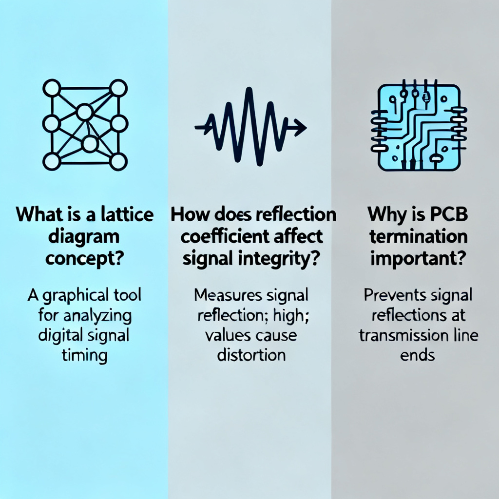
What is the Lattice Diagram Method used for in high-speed PCB design?
The Lattice Diagram Method visualizes voltage and current wave reflections along a transmission line, helping engineers optimize impedance control and termination for high-speed PCB.
How does the Lattice Diagram Method help with impedance matching?
By tracking each reflected wave, the Lattice Diagram Method shows how mismatched impedances at source or load cause multiple reflections, guiding termination resistor selection for your custom high-speed PCB.
Can the Lattice Diagram Method handle lossy transmission lines?
The basic Lattice Diagram Method assumes lossless lines. For lossy high-speed PCB materials, use simulation tools that incorporate frequency-dependent attenuation.
What is the difference between Lattice Diagram Method and TDR?
Time-Domain Reflectometry (TDR) is a measurement technique, while the Lattice Diagram Method is an analytical tool. Both rely on the same wave reflection principles for high-speed PCB signal integrity.
How many reflections should I track in a Lattice Diagram Method?
Continue the Lattice Diagram Method until reflected wave amplitude drops below 1% of the initial wave. For typical high-speed PCB designs, 5-10 reflections suffice.
7. Conclusion: Integrating Lattice Diagram Method into Your PCB Workflow
The Lattice Diagram Method is an essential analytical tool for any high-speed PCB engineer. By visually mapping voltage wave journeys, it demystifies reflection behavior and empowers informed decisions about impedance control, termination, and topology. For B2B PCB manufacturing and custom high-speed boards, mastering this technique ensures your designs meet stringent signal integrity requirements, reducing costly prototype iterations.
Ready to build your next high-speed PCB? Our engineering team can help you simulate, optimize, and fabricate boards with guaranteed impedance control and minimal reflections.