In modern high-speed PCB design, mastering the power integrity hierarchy of on-die, package, and PCB decoupling is essential for suppressing noise, reducing EMI, and ensuring signal integrity in advanced digital systems. As clock frequencies rise into the gigahertz range and supply voltages drop below 1V, the margin for voltage ripple shrinks dramatically. A failure in decoupling can lead to timing errors, data corruption, or complete system malfunction.
Power Integrity Fundamentals and Decoupling
What is Decoupling and Why Does It Matter in High-Speed PCB Design?
Decoupling (or bypass) capacitors serve two primary functions in the power integrity hierarchy: they provide local energy storage to prevent voltage droop during transient current draws, and they create a low-impedance path to ground for high-frequency AC noise. Without proper decoupling, the PDN impedance can spike at specific frequencies, causing voltage ripple that violates the IC’s supply tolerance.
The Impedance Target: Foundation of PDN Design
The most critical metric in PDN design is the target impedance (Z_target). For a 1.2V rail with 3% tolerance and 10A transient current, Z_target = (1.2 × 0.03) / 10 = 3.6 mΩ. Achieving such low impedance across a wide frequency range requires multiple decoupling layers working in concert within the power integrity hierarchy.
The Self-Resonant Frequency and Anti-Resonance
Every capacitor has a self-resonant frequency (SRF) where its impedance is minimum. When multiple capacitors with different values are placed in parallel, their impedance curves combine. If the SRFs are too close, an anti-resonance peak can occur—a spike in impedance that amplifies noise rather than suppressing it. This is a critical consideration in the power integrity hierarchy.
On-Die Decoupling Capacitance: The First Line of Defense
How On-Die Capacitance Fits in the Power Integrity Hierarchy
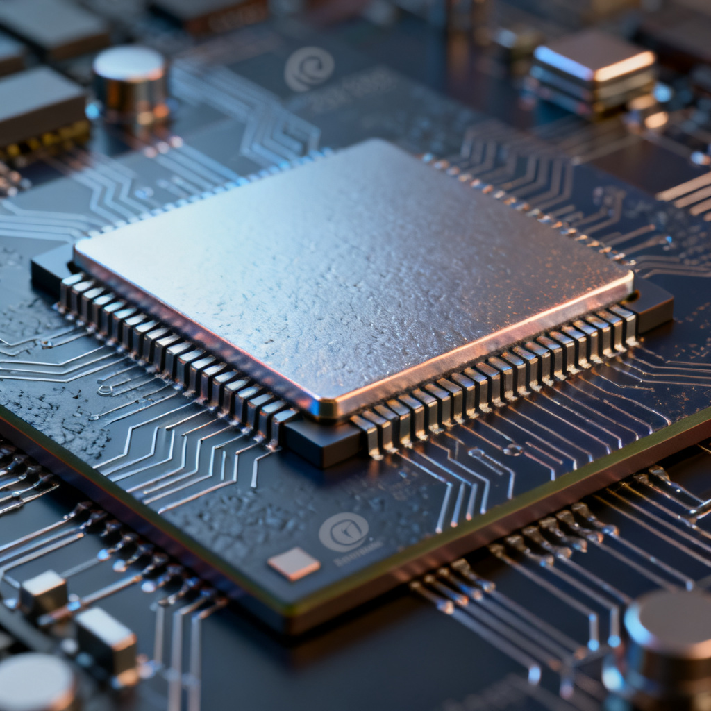
On-die decoupling capacitance (ODC) is the capacitance integrated directly into the silicon die, operating in the GHz range from approximately 100 MHz to 10+ GHz. It is the highest-frequency decoupling layer and the closest to the switching transistors, typically implemented as MOS capacitors, MIM capacitors, or deep trench capacitors.
Frequency Response and Impedance of On-Die Decoupling
ODC provides extremely low impedance at high frequencies because the physical distance from the transistors is measured in micrometers, minimizing parasitic inductance. A typical high-performance processor might integrate tens to hundreds of nanofarads of ODC. However, ODC has limited capacitance density, leakage current issues, and voltage sensitivity, making it insufficient alone for the power integrity hierarchy.
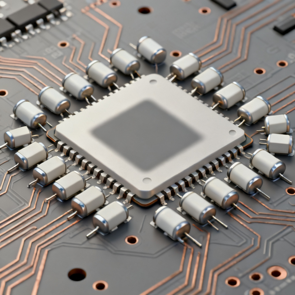
Package-Level Decoupling Capacitors: Bridging the Gap
The Role of Package Decoupling in the Power Integrity Hierarchy
Package-level decoupling capacitors are discrete components mounted on the IC package substrate, operating in the 10 MHz to 1 GHz range. They serve as the intermediate tier between the ultra-fast on-die capacitance and the slower PCB decoupling. Common types include X7R and X5R MLCCs for bulk capacitance, C0G/NP0 MLCCs for low ESL, and embedded capacitors for even lower inductance.
Design Guidelines for Package Decoupling
High-performance packages may use 20–100+ MLCCs. Capacitors should be placed within 2–5 mm of the die power pads to minimize loop inductance. Use a mix of values spaced by a factor of 10–100 in capacitance to avoid anti-resonance, or use many identical low-ESL capacitors for a broad, flat impedance curve. Some package capacitors are intentionally chosen with higher ESR to dampen anti-resonance with ODC or PCB capacitors.
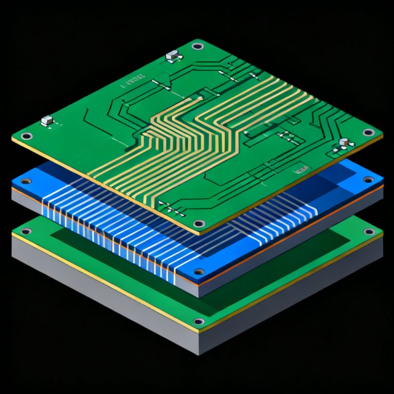
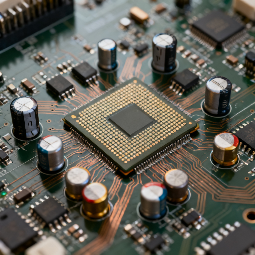
PCB-Level Decoupling Capacitors: The Workhorse
PCB Decoupling in the Power Integrity Hierarchy
PCB-level decoupling capacitors provide bulk energy storage for the entire PDN and filter noise from DC up to tens of megahertz. They are the most common tier, typically MLCCs mounted near the power pins of ICs. The limiting factor is the parasitic inductance of PCB traces, vias, and the capacitors themselves, which sets the SRF at a much lower frequency than package capacitors.
Types of PCB Decoupling Capacitors
| Capacitor Type | Value Range | Frequency Range | Role in Power Integrity Hierarchy |
|---|---|---|---|
| Bulk Capacitors | 10 µF to 1000 µF | 1 Hz to 1 MHz | Main charge reservoir for low-frequency transients |
| Mid-Frequency Capacitors | 0.1 µF to 10 µF | 1 MHz to 10 MHz | Most common decoupling capacitors |
| High-Frequency Capacitors | 10 pF to 100 nF | Up to 50–100 MHz | Very low ESL and ESR for high-frequency filtering |
PCB Decoupling Design Best Practices
Place capacitors around the entire perimeter of the IC to minimize loop area. Use multiple vias per capacitor to reduce effective inductance. Maximize planar capacitance between power and ground planes by using thin dielectrics. Follow the “decade spacing” rule or use many identical small-value capacitors for predictable impedance. For bulk capacitors, choose types with higher ESR to dampen low-frequency anti-resonance.
Integration of the Three Tiers in the Power Integrity Hierarchy
The Impedance Curve: A Visual Guide
The power integrity hierarchy can be visualized as a series of impedance curves: on-die provides lowest impedance above 1 GHz, package provides lowest impedance from 10 MHz to 1 GHz, and PCB plus VRM provides lowest impedance from DC to 10 MHz. The goal is to have the combined impedance stay below Z_target across the entire frequency range.
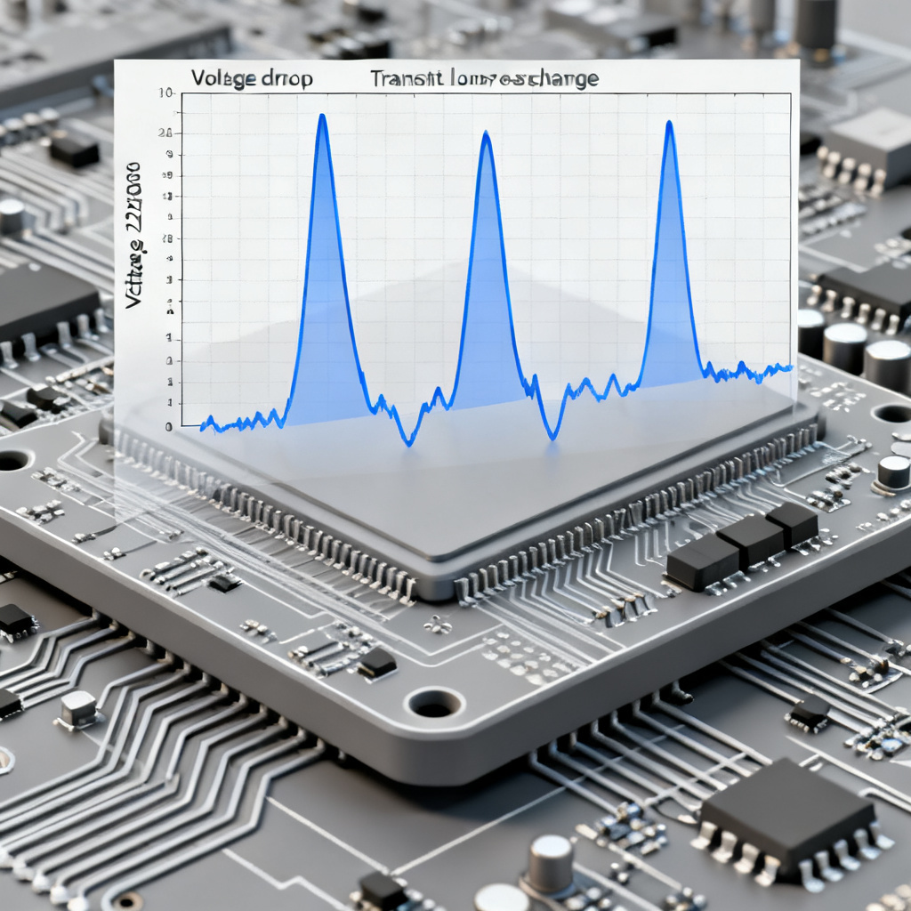
Anti-Resonance: The Hidden Danger
Anti-resonance occurs when the impedance curves of two decoupling layers overlap, creating a peak. Mitigation strategies include using capacitors with different ESR values, adding a small resistor in series, using many identical capacitors, and simulating the PDN with tools like ANSYS SIwave, Cadence Sigrity, or Keysight ADS.
Practical Design Flow for Power Integrity Hierarchy
Determine Z_target from the IC datasheet. Model the ODC from the IC vendor. Design the package decoupling using the package substrate layout guidelines. Design the PCB decoupling starting from the VRM output. Iterate until the combined impedance is below Z_target across all frequencies. Simulation is not optional for modern high-speed designs.
Advanced Topics and Emerging Trends
Embedded Capacitors in PCB
Some advanced PCBs use embedded capacitors—thin layers of high-dielectric-constant material laminated into the PCB stackup. These provide distributed capacitance with extremely low ESL (10–50 pH), making them effective up to 10 GHz. However, they are expensive and require specialized manufacturing.
Active Decoupling and On-Chip Regulation
For extremely demanding applications, designers are turning to Fully Integrated Voltage Regulators (FIVR) that integrate the VRM function onto the die, reducing the need for external decoupling and allowing per-core voltage scaling.
The Impact of 3D Packaging and Chiplet Architectures
In 3D-ICs and chiplet-based designs, the decoupling hierarchy becomes more complex. Interposers add another layer of capacitance between the die and the package. The PDN must be modeled across all three dimensions, and thermal effects become significant.
Material Selection for MLCCs
Class 1 (C0G/NP0) offers stable capacitance over temperature and voltage, ideal for high-frequency decoupling. Class 2 (X7R, X5R) provides high capacitance density but capacitance drops with DC bias and temperature. Class 3 (Y5V, Z5U) offers very high capacitance but poor stability and should be avoided in precision designs.
Frequently Asked Questions About the Power Integrity Hierarchy
What is the power integrity hierarchy in high-speed PCB design?
The power integrity hierarchy refers to the three tiers of decoupling: on-die capacitance, package-level decoupling, and PCB-level decoupling. Each tier addresses a different frequency range and impedance target, working together to deliver clean power to active devices.
How do I choose the right decoupling capacitors for my power integrity hierarchy?
Start by determining the target impedance from the IC datasheet. Then select capacitor values that cover the frequency range from DC to the highest harmonic of the switching frequency. Use a mix of bulk, mid-frequency, and high-frequency capacitors, and simulate the entire PDN to avoid anti-resonance.
Why is anti-resonance a concern in the power integrity hierarchy?
Anti-resonance creates a high-impedance peak that amplifies noise rather than suppressing it. This can cause voltage ripple that violates the IC’s supply tolerance, leading to timing errors or system malfunction. Proper capacitor value spacing and ESR selection help mitigate this risk.
What tools are used for power integrity hierarchy simulation?
Common tools include ANSYS SIwave, Cadence Sigrity, and Keysight ADS. These tools allow designers to plot impedance vs. frequency, identify anti-resonance peaks, optimize capacitor placement, and model the effect of PCB stackup.
How does the VRM fit into the power integrity hierarchy?
The VRM is the ultimate source of power for the PDN but typically has a bandwidth of 1–10 kHz. Below this frequency, the VRM’s output impedance is low; above it, the VRM becomes inductive. The PCB decoupling capacitors must handle everything above 10 kHz.
Power Integrity Hierarchy: On-Die, Package, and PCB Decoupling Services
We provide expert design and manufacturing services for high-speed PCB systems requiring optimized power integrity hierarchy. Our offerings include PDN simulation, decoupling capacitor selection, and custom PCB fabrication with controlled impedance stackups. Each project is tailored to meet your target impedance requirements across all three decoupling tiers.