Power Integrity PCB is equally important as signal integrity for modern high-speed circuits. This guide introduces full PDN analysis workflows via Keysight ADS to solve voltage ripple, jitter and intermittent bit errors on PCBs.
1. Why Power Integrity PCB Matters in High-Speed Design
Unstable power supply directly destroys the performance of high-speed digital PCBs. “It takes only one rogue voltage wave to kill a power distribution network.” In modern digital systems, failures of Power Integrity PCB are increasingly the root cause of signal integrity problems—not the other way around.
1.1 The Hidden Problem
Voltage tolerance of high-speed chips is very strict and vulnerable to PDN noise. Consider this: A DDR4 memory interface operates at 1.2V with a typical ripple tolerance of just ±5% (60mV). A 1.0V core voltage for a high-performance processor allows only 50mV of noise. When your power distribution network introduces voltage ripple, the effects cascade:
| PI Problem | SI Consequence | System Impact |
|---|---|---|
| Power supply ripple | Increased jitter | Timing violations |
| Ground bounce | Reduced noise margin | Bit errors |
| PDN resonance | Eye diagram closure | Reduced data rate |
| IR drop | Logic threshold drift | Intermittent failures |
Most signal faults are actually hidden power integrity defects. The reality: Many PCB failures diagnosed as “signal integrity issues” are actually Power Integrity PCB problems in disguise. A poorly designed power distribution network causes ground bounce, increases jitter by 100 ps/mV, and closes the eye diagram—manifesting as bit errors that are incredibly difficult to debug without proper simulation tools.
1.2 Why Choose Keysight ADS for Simulation
Keysight ADS is the industry-standard EDA tool for high-speed PCB simulation. Keysight ADS is the industry gold standard for high-speed digital design, offering:
- Native integration with Keysight measurement instruments (VNAs, oscilloscopes)
- Unified platform for RF and high-speed digital design
- PIPro module specifically designed for complete Power Integrity PCB analysis
- Automated decoupling capacitor optimization that no other tool matches
2. PDN Fundamentals for Power Integrity PCB
Master basic PDN concepts before starting professional simulation work. Before diving into simulation steps, let‘s establish the essential concepts. If you‘re already familiar, use this section as a quick refresher.
2.1 The Three Layers of power distribution network
A complete power distribution network consists of three interconnected domains:
┌─────────────┐     ┌─────────────┐     ┌─────────────┐
│    VRM      │────▶│  PCB PDN    │────▶│   On-chip   │
│  (Voltage   │     │ (Planes,    │     │   PDN       │
│  Regulator) │     │  Vias,      │     │ (Capacitance│
└─────────────┘     │  Traces)    │     │  Package)   │
                    └─────────────┘     └─────────────┘
                     ↑                          ↑
                Low frequency              High frequency
2.2 The Three Analysis Dimensions
| Analysis Type | Question It Answers | Key Metric |
|---|---|---|
| DC IR Drop | How much voltage is lost from VRM to load? | <2–3% of nominal voltage |
| AC Impedance | How does PDN impedance vary with frequency? | target impedance |
| Transient Response | How does voltage respond to sudden load changes? | Overshoot/Undershoot |
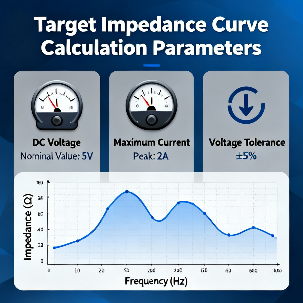
2.3 target impedance – The Critical Equation
Use the standard formula to calculate the core index of PDN design. For engineers who want the technical depth:
$$Z_{target} = \frac{V_{rail} \times \text{Ripple}\%}{I_{transient}}$$
Example calculation:
- Vrail = 1.2V (DDR4 VDDQ)
- Ripple tolerance = 5% = 0.06V
- Itransient = 2A (sudden current draw)
- Ztarget = 30 mΩ
This means: Your power distribution network must maintain impedance below 30 mΩ from DC to hundreds of MHz. Any peak above 30 mΩ indicates potential voltage ripple violations during transient events.
2.4 How PI Problems Manifest as signal integrity Issues
Power noise is the main inducement of signal distortion. “Power integrity issues don‘t just cause power problems—they create signal integrity failures that look like something else entirely.”
- PDN impedance peak at certain frequency
- Load current at that frequency causes voltage ripple
- Ripple modulates signal timing (jitter)
- Jitter reduces eye opening
- Bit error rate increases
The math: Typical industry data shows 100 ps of jitter per millivolt of power supply ripple.
3. Keysight ADS PI Analysis Toolchain Overview
Understand tool modules to select correct functions for PDN analysis. Keysight ADS provides a comprehensive suite for Power Integrity PCB analysis. Here‘s what each module does:
3.1 Core Tools
| Module | Function | Best For |
|---|---|---|
| PIPro | PDN DC/AC analysis, plane resonance, decap optimization | Complete PI workflow for Power Integrity PCB |
| SIPro | Signal net EM extraction | S-parameter extraction for high-speed signals |
| Electrothermal | Coupled thermal-electrical simulation | High-current designs (>50A) |
3.2 What Makes Keysight ADS Different?
| Feature | ADS Advantage |
|---|---|
| Instrument integration | Direct import of VNA measurements to calibrate simulation models |
| PI Advisor | Automated decoupling capacitor optimization |
| Hybrid solver | Combines EM and circuit simulation for accuracy + speed |
| Design synchronization | Changes in layout automatically update simulation |
3.3 Prerequisites for This Guide
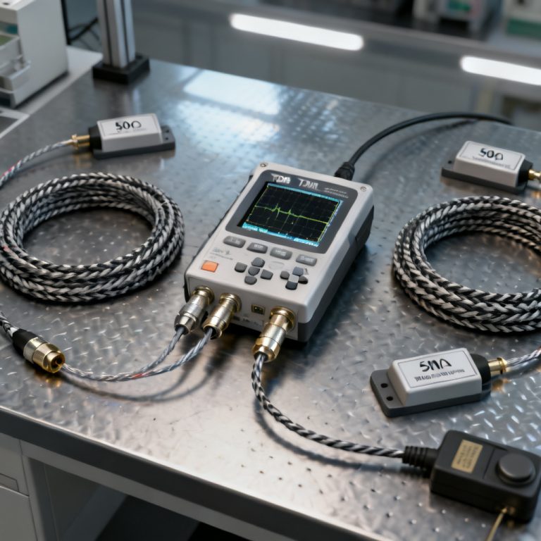
Prepare files and models before running simulation. To follow along, you’ll need:
- Keysight ADS with PIPro license (evaluation license available from Keysight)
- A PCB layout file (ODB++, IPC-2581, or native formats from Allegro, Altium, Mentor)
- Component models (VRM S-parameters, capacitor S-parameters from manufacturers)
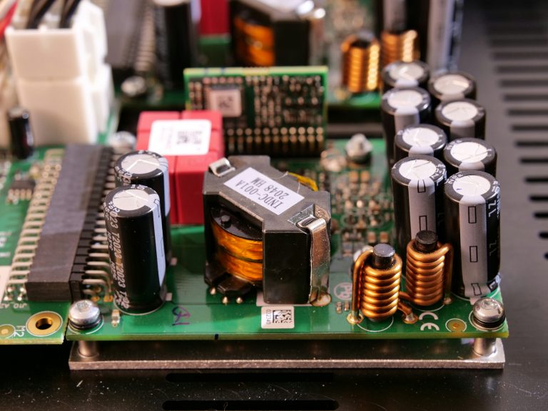
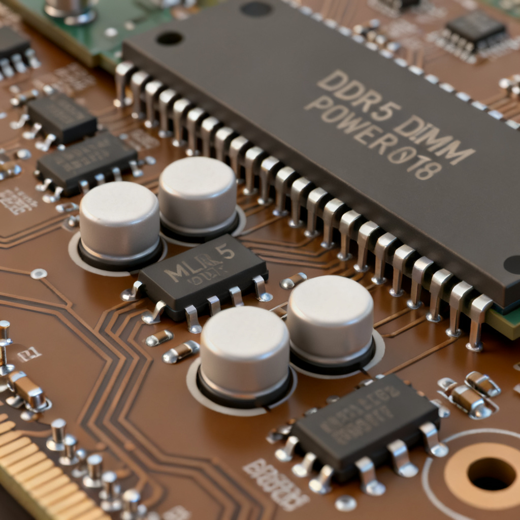
4. Step 1: Complete PCB layout import into ADS
Accurate layout import is the premise of reliable simulation results. The first step is getting your PCB design into ADS. Accuracy here is critical—garbage in, garbage out for reliable Power Integrity PCB simulation results.
4.1 Supported File Formats
| Format | Recommended? | Why |
|---|---|---|
| ODB++ | ✅ Highly recommended | Preserves stackup, padstacks, and netlist completely |
| IPC-2581 | ✅ Good | Modern standard with good fidelity |
| Allegro .brd | ✅ Native support | Direct import if using Cadence |
| Altium .pcbdoc | ✅ Via ODB++ export | Export from Altium first |
4.2 Post-Import Validation Checklist
After import, always verify these three items before running simulations:
✅ Stackup Verification
Layer thickness matches your fabrication drawing
Copper weight (1oz, 2oz, etc.) is correct
Material Dk/Df values are accurate for your frequency range
✅ Padstack Verification
Via barrel dimensions
Antipad clearance (critical for plane coupling)
Thermal relief spoke width
✅ Component Model Assignment
VRM: S-parameter or SPICE model (not ideal voltage source!)
Load ICs: PDN model from vendor or current profile
Decoupling capacitors: S-parameter models from manufacturer
4.3 Pro Tip – The VRM Modeling Trap
Ideal voltage source will cause large simulation deviation. “Using an ideal voltage source for VRM modeling is the #1 mistake in PI simulation. It completely misses low-frequency PDN characteristics below 1 MHz.”
Always use a realistic VRM model with output impedance characteristics. Most VRM vendors provide S-parameter models or can generate them upon request.
5. Step 2: Run DC IR Drop simulation
DC IR Drop simulation checks static voltage loss on PCBs. What it answers: “How much voltage actually reaches my IC?” DC IR Drop analysis is the first line of defense in Power Integrity PCB design. It identifies DC voltage losses due to trace and plane resistance.
5.1 Setting Up Your Simulation
| Setup Item | What to Specify | Example |
|---|---|---|
| Source (VRM) | Output voltage, current capability | 1.2V, 5A max |
| Sink (Load) | Current draw per pin/region | 2A at FPGA core |
| Sense point | Where to measure voltage | IC power pin |
5.2 Running the Simulation
- Navigate to PIPro → DC Analysis → IR Drop
- Assign voltage sources to VRM output nets
- Assign current sinks to load device pins
- Set convergence options (start with default)
- Run simulation
5.3 Interpreting Results
Two core visualization results help locate design bottlenecks. ADS generates several visual outputs:
Voltage Distribution Color Map
Red regions indicate highest voltage drop
Green/blue regions show healthy voltage levels
Sharp transitions indicate bottlenecks
Current Density Map
Hotspots show areas exceeding copper current capacity
Industry rule of thumb: ~50A/mm² for 1oz copper with 10°C rise
Real design case: “In a PCIe 5.0 design, the 0.8V rail was analyzed using ADS PIPro. The simulation identified a 150mV drop in the ground return path—three times the drop in the power trace. The root cause was a ground plane necking down to 15 mils between two mounting holes. Widening the passage reduced the return path resistance by 60%.”
5.4 Acceptance Criteria
| Design Type | Maximum IR Drop |
|---|---|
| General purpose | <5% of Vnom |
| High-performance digital | <3% of Vnom |
| Sensitive analog/RF | <1% of Vnom |
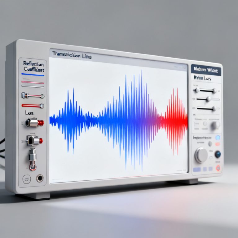
6. Step 3: Run AC impedance simulation
AC impedance simulation is the core of full-band PDN testing. What it answers: “Does my PDN maintain impedance below target impedance across all frequencies?” This is the heart of Power Integrity PCB analysis. While DC analysis looks at resistance, AC analysis examines impedance across frequency—where most PDN failures occur.
6.1 Setting Up AC Ports
| Port Type | Location | Purpose |
|---|---|---|
| Source port | VRM output | Inject stimulus |
| Load port | IC power pin | Observe response |
| Component ports | Decoupling capacitors | Include their effects |
6.2 Understanding the Z-Parameter Curve

A typical PDN impedance curve shows three regions:
Impedance (log scale)
     ↑
     │                                    Ztarget ─────────
     │        VRM      │  Bulk Caps  │ Ceramic │ Plane │ On-chip
     │      Dominant   │  Dominant   │ Caps Dom│ Cap Dom│ Cap Dom
     │    ────────┐    │    ┌───┐    │   ┌─┐   │  ┌─┐  │  ┌─┐
     │           │    │  ┌─┘   └─┐  │ ┌─┘ └─┐ │┌┘ └┐│ │┌┘ │
     │───────────┴────┴──┴───────┴──┴─┴─────┴─┴┴───┴┴─┴──┴──▶ Frequency
        10Hz    1kHz   100kHz   10MHz   100MHz   1GHz   10GHz
6.3 The target impedance Check
Impedance peaks mean potential resonance and noise amplification. The rule: PDN impedance must stay below target impedance across the entire frequency range of interest.
What impedance peaks mean:
A peak indicates a resonance between parasitic inductance and capacitance
At that frequency, the PDN will amplify noise instead of suppressing it
Transient current at that frequency will cause voltage ripple exceeding Ztarget × Itransient
6.4 Common Impedance Peak Locations and Causes
| Frequency Range | Typical Cause | Fix |
|---|---|---|
| 100kHz – 1MHz | Gap between VRM and bulk caps | Add bulk capacitance |
| 1MHz – 50MHz | Inadequate ceramic decoupling | Add more/appropriate MLCCs |
| 50MHz – 200MHz | Mounting inductance too high | Reduce via distance, use smaller packages |
| >200MHz | Plane resonance | Adjust plane shape, add stitching caps |
7. Step 4: Complete decoupling capacitor optimization
decoupling capacitor optimization is the core optimization step for PDN. This is where Keysight ADS PIPro truly shines. The PI Advisor feature automates what used to be a manual, iterative, and error-prone process for stable Power Integrity PCB.
7.1 The Flat Impedance Design Philosophy
Traditional approach: Add capacitors at peaks until impedance drops below target impedance.
Modern approach (Keysight-recommended): Design for flat impedance across frequency.
Why flat impedance matters:
- Predictable PDN behavior regardless of load current spectrum
- No unexpected resonances from “over-decoupling”
- Lower part count when optimized correctly
7.2 Using ADS PI Advisor
- Define target impedance mask – Draw your Ztarget line across frequency
- Select capacitor library – Choose from manufacturer databases (Murata, TDK, Samsung, etc.)
- Set constraints – Maximum part count, preferred packages (e.g., 0402 preferred, 0201 allowed)
- Run optimization – PI Advisor tests millions of combinations
- Review solution – Compare before/after impedance curves
7.3 Critical Insight – Mounting Inductance
“A 0402 capacitor mounted with improper via placement can have 2-3× higher inductance than its datasheet suggests, shifting its effective frequency range downward significantly.”
Mounting inductance formula: $$L_{mount} \approx \frac{2 \times \text{loop area}}{\text{via spacing}}$$
Layout best practices:
Place vias as close to capacitor pads as possible
Use multiple vias per capacitor (2 minimum, 4 better)
Avoid shared vias between capacitors (via starvation)
ADS advantage: PIPro can extract mounting inductance from layout geometry, giving you accurate effective capacitance, not just idealized component models.
7.4 Before vs. After – What to Expect
| Metric | Before Optimization | After Optimization |
|---|---|---|
| Peak impedance | 85 mΩ at 3.2 MHz | 28 mΩ at all frequencies |
| Decap count | 24 | 18 |
| Voltage ripple @ 2A transient | 170 mV (14% of 1.2V) | 56 mV (4.7% of 1.2V) |
8. Step 5: Advanced electrothermal analysis
electrothermal analysis is required for high-current PCB designs. For high-current designs—AI accelerators, GPU servers, automotive power distribution—thermal effects cannot be ignored for reliable Power Integrity PCB.
8.1 Why Thermal Matters for Power Integrity
Three effects create a dangerous positive feedback loop:
$$\text{IR Drop} \rightarrow \text{Local Heating} \rightarrow \text{Increased Copper Resistance} \rightarrow \text{More IR Drop} \rightarrow (\text{repeat})$$
The physics: Copper has a temperature coefficient of resistance (TCR) of approximately 0.4% per °C. A 50°C temperature rise increases copper resistance by 20%, worsening IR drop significantly.
8.2 ADS Electrothermal Workflow
- Define thermal properties – Copper thermal conductivity (~400 W/m·K), FR4 conductivity (~0.3 W/m·K)
- Set boundary conditions – Ambient temperature, airflow, heatsink attachment
- Run DC simulation – Get power dissipation distribution
- Run thermal simulation – Get temperature distribution
- Iterate – Update resistance based on temperature, repeat until convergence
8.3 When You Need electrothermal analysis
| Application | Current per rail | Electrothermal Required? |
|---|---|---|
| Smartphone | <5A | Usually not |
| Laptop | <20A | Optional |
| Server CPU | 100-300A | ✅ Yes |
| GPU/AI accelerator | 500-2000A+ | ✅ Mandatory |
9. Interpreting Results and Generating Reports
Standard reports help docking design, testing and PCB manufacturing. After simulation, you need to communicate results clearly—to your manager, your customer, or your fabrication partner to guarantee qualified Power Integrity PCB.
9.1 Professional Report Template
- Design Information: Board name and revision, stackup table, power nets analyzed
- DC IR Drop Results: Maximum IR drop, location screenshot, pass/fail status
- AC Impedance Results: Impedance curve plot, peak values, pass/fail status
- Decoupling Capacitor Solution: Final BOM, placement guidelines, comparison chart
- Conclusions and Recommendations: Defect summary, revision suggestions, fabrication risk assessment
9.2 Example Pass/Fail Summary Table
| Power Rail | Vnom | Ztarget | Max IR Drop | Max Impedance | Overall |
|---|---|---|---|---|---|
| VDDQ_DDR4 | 1.2V | 30 mΩ | 18 mV (1.5%) | 28 mΩ | ✅ PASS |
| VCCORE | 1.0V | 25 mΩ | 35 mV (3.5%) | 42 mΩ | ❌ FAIL |
| VCCIO | 3.3V | 80 mΩ | 45 mV (1.4%) | 65 mΩ | ✅ PASS |
10. From Simulation to PCB manufacturing
Simulation results must match actual PCB manufacturing capabilities. This is where your PCB manufacturing partner matters. Power Integrity PCB analysis identifies what your design needs. But simulation results are only valuable if your PCB fabricator can deliver those requirements.
10.1 Manufacturing Requirements Derived from PI Analysis
| PI Requirement | Manufacturing Implication |
|---|---|
| Tight impedance control (±10%) | Controlled dielectric thickness, etch compensation |
| Low-inductance capacitor mounting | Via-in-pad with fill and cap |
| High current capacity (2oz+ copper) | Heavy copper capabilities |
| Thin dielectric for plane coupling | Advanced lamination press |
| Low-loss material (Megtron 6, etc.) | Materials procurement capability |
10.2 What to Ask Your PCB Manufacturer
Before sending your design to fabrication, verify:
- ✓ Impedance control tolerance – Can they hold ±10% on 50Ω traces?
- ✓ Via-in-pad capability – Do they offer filling (copper or non-conductive)?
- ✓ Heavy copper – What‘s their maximum copper weight (2oz, 3oz, 4oz+)?
- ✓ Material availability – Do they stock low-loss materials (Rogers, Megtron, Isola)?
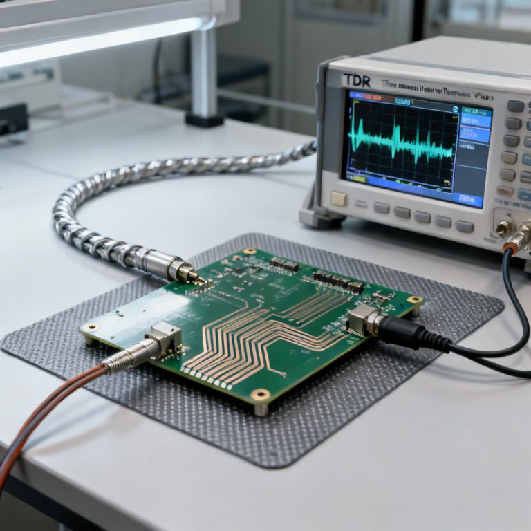
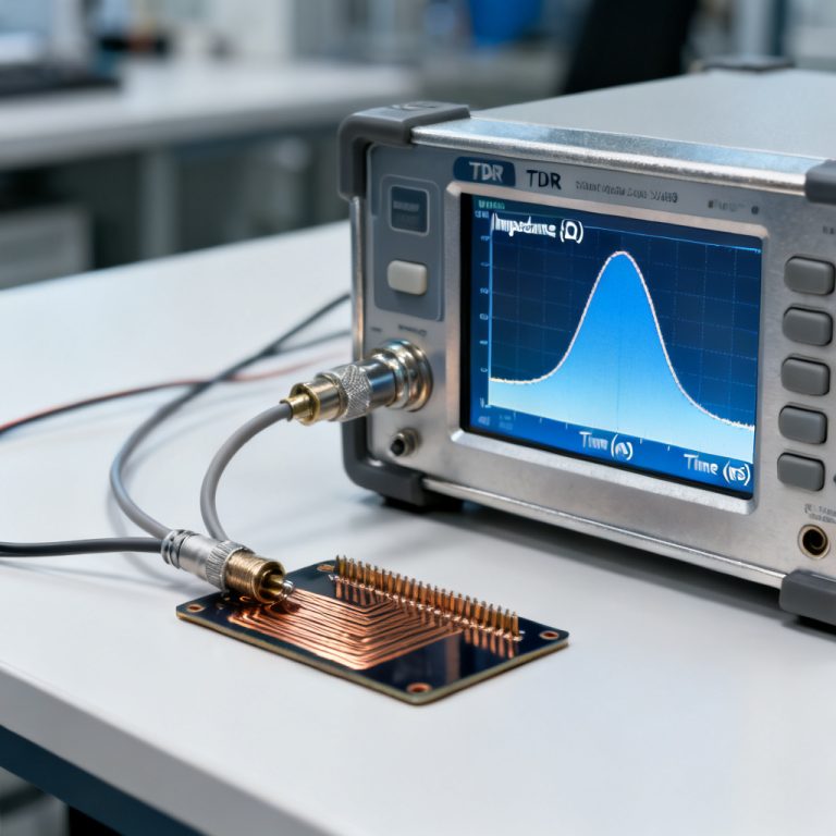
- ✓ Testing – Do they provide impedance test coupons and report?
10.3 Manufacturing Capability Reference
| Your PI Requirement | Our Capability |
|---|---|
| ±10% impedance control | Standard process, TDR verified |
| Via-in-pad with filling | Copper-filled or resin-filled |
| Up to 6oz copper | Heavy copper production line |
| Low-loss materials | Rogers, Megtron 6, Isola in stock |
| 20+ layer stackups | HDI and high-layer count capability |
| Comprehensive testing | Impedance, IR drop, flying probe, X-ray |
We don’t just read your simulation report—we build to it.
11. Frequently Asked Questions (FAQ)
Q1: What‘s the difference between Power Integrity PCB and signal integrity?
A: Think of it this way: signal integrity ensures signals get from point A to point B cleanly. Power Integrity PCB ensures the power distribution network delivers stable voltage so signals can be clean. In practice, PI problems (like ground bounce) directly cause signal integrity problems (like increased jitter and eye closure).
Q2: Do I always need full PDN analysis for every design?
A: No. The level of analysis should match design complexity:
- Simple 2-layer boards (<50MHz) – Rule-of-thumb decoupling is often sufficient
- 4-6 layer mixed-signal – DC IR Drop analysis recommended
- High-speed digital (DDR, PCIe, SERDES) – Full PI-AC analysis required
- AI/GPU/server boards – electrothermal analysis recommended
Q3: How accurate are PI simulations compared to real measurements?
A: With proper models (accurate VRM S-parameters, capacitor models with mounting inductance), Keysight ADS simulations typically achieve 10-15% correlation with VNA measurements. The gap comes from unknown IC PDN models, manufacturing variations and PCB assembly variations.
Q4: What‘s the best decoupling capacitor strategy for wideband PDN?
A: The Keysight-recommended “flat impedance“ approach:
- Low frequency (10kHz-1MHz) – VRM output capacitors (electrolytic or polymer)
- Mid frequency (1MHz-50MHz) – Bulk ceramic (10µF to 100µF, 0805/1206)
- High frequency (50MHz-500MHz) – Small MLCCs (0.1µF to 1µF, 0402/0201)
- Very high frequency (>500MHz) – Power-ground plane capacitance (thin dielectrics)
Q5: How long does a typical PI simulation take?
A:
- DC IR Drop simulation: 5-15 minutes setup, 2-10 minutes simulation
- AC impedance simulation (full PDN): 30-60 minutes setup, 5-30 minutes simulation
- With decoupling capacitor optimization: Additional 10-30 minutes of compute time
- electrothermal analysis: 1-2 hours for convergence
Q6: Can I run PI simulation without a full PCB layout import?
A: Yes, for early design phases:
- Pre-layout assessment – Use PDN impedance calculators with estimated parasitics
- Floorplanning – Identify VRM-to-load distances, plane splits
- Capacitor planning – Generate target impedance curves and capacitor selection
However, final verification requires full layout extraction.
Q7: What‘s the #1 mistake engineers make in PI simulation?
A: Using ideal components. Three specific traps:
- Ideal VRM voltage source (misses low-frequency behavior)
- Ideal capacitor models (ignores ESL and mounting inductance)
- Ignoring via antipads (affects plane-to-plane coupling)
Always use S-parameter models for VRM and capacitors when available.
12. Next Steps & Expert Support
You now have a complete workflow for power integrity analysis using Keysight ADS to achieve reliable Power Integrity PCB performance. But analysis is only half the story—PCB manufacturing is where theory meets reality.