Understanding how solder mask and surface finish create minor reflections in transmission line is critical for high-speed PCB signal integrity. These subtle impedance discontinuities, often below -20 dB, accumulate in 10+ Gbps designs, degrading eye diagrams and increasing bit error rates. This guide consolidates expert engineering insights to help you mitigate these effects.
The Physics of How Solder Mask and Surface Finish Create Minor Reflections in Transmission Line
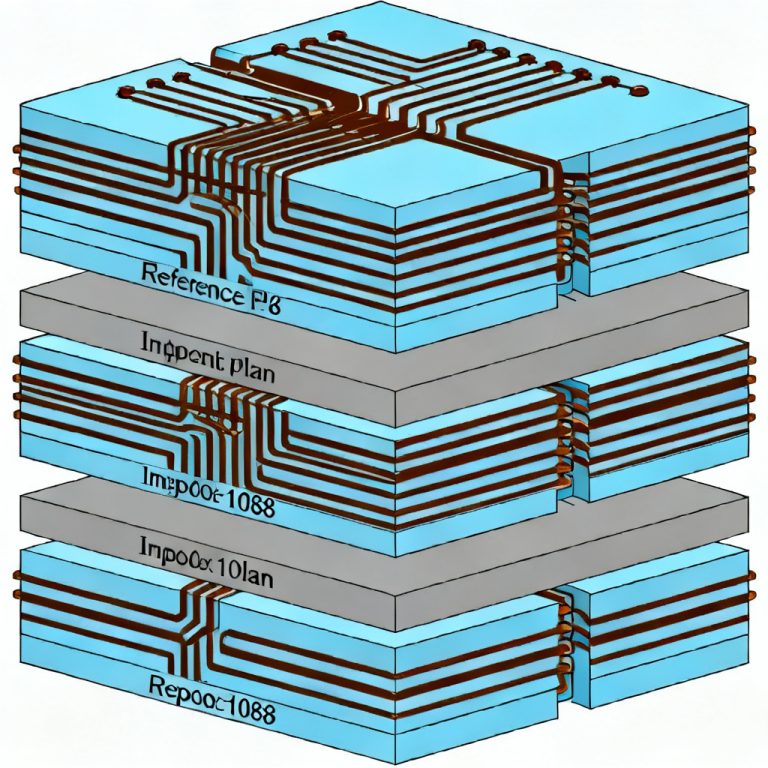
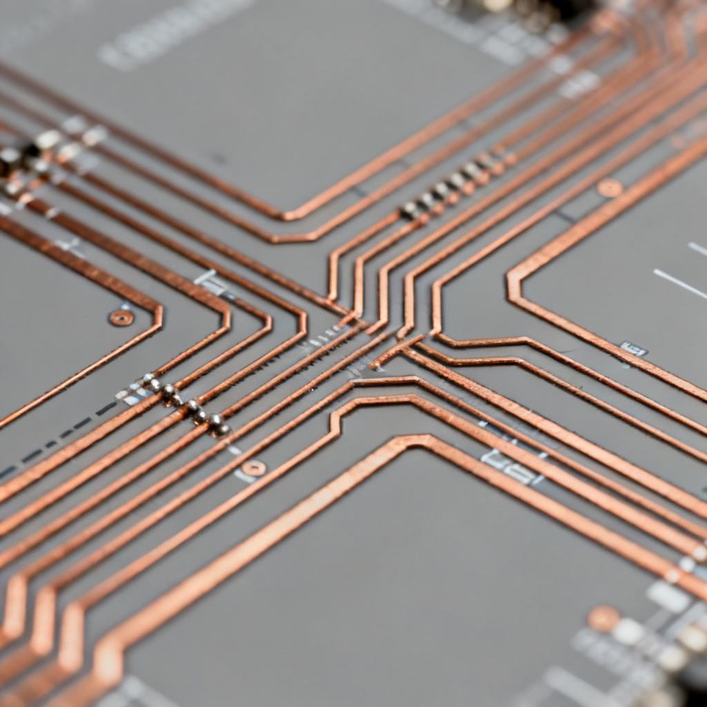
1.1 What Are Minor Reflections in Transmission Line?
Minor reflections in transmission line are small impedance discontinuities caused by local changes in characteristic impedance (Z0). When a signal encounters a region with altered dielectric constant (εr) or conductor geometry, a fraction of energy is reflected. For solder mask and surface finish, these reflections are typically below -20 dB but can cause cumulative jitter in long traces or high-speed buses.
1.2 How Solder Mask Alters Impedance and Creates Minor Reflections in Transmission Line
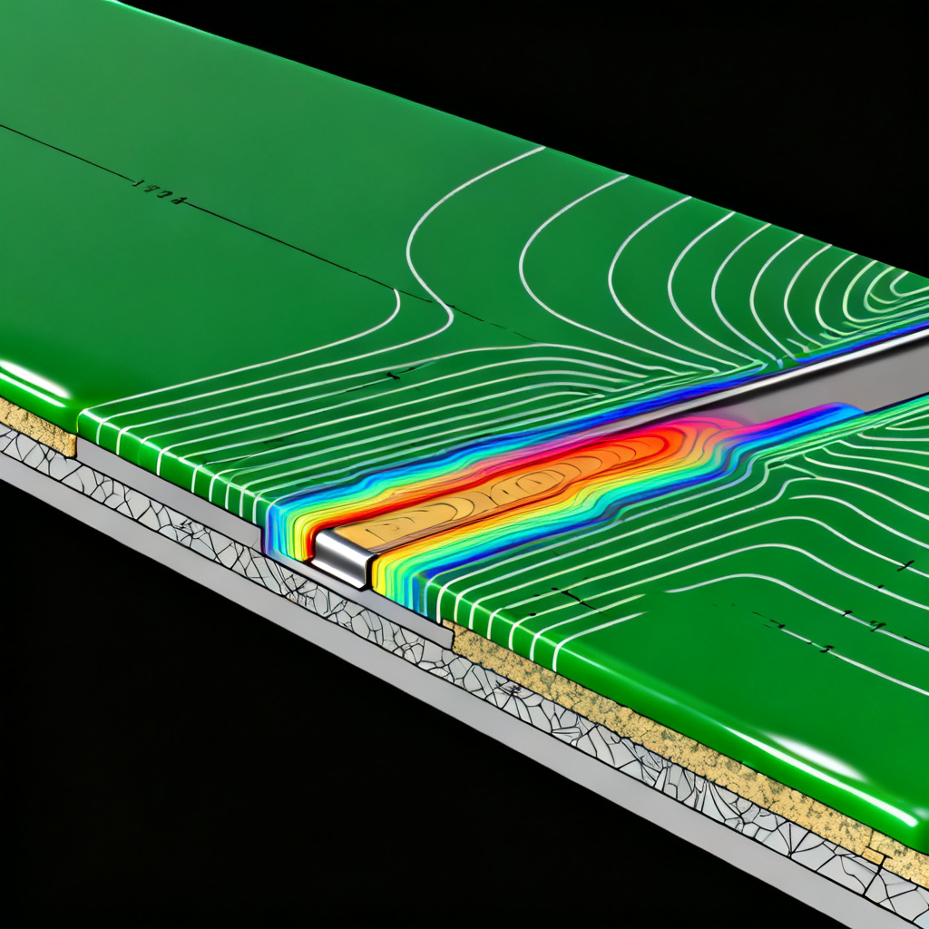
Solder mask is a dielectric coating applied over copper traces. Its permittivity (εr ≈ 3.0–4.5) and thickness (typically 0.5–1.5 mils) change the effective dielectric constant around the trace, modifying capacitance per unit length and shifting Z0. This is a primary mechanism of how solder mask and surface finish create minor reflections in transmission line.
- Increase in εr: Solder mask raises effective εr, lowering Z0 by 1–5 ohms.
- Non-uniform coverage: Variations in solder mask thickness create localized impedance dips.
- Frequency dependence: At GHz frequencies, solder mask loss tangent (tan δ ≈ 0.015–0.03) adds attenuation and phase distortion.
1.3 How Surface Finish Affects Signal Propagation and Creates Minor Reflections in Transmission Line
Surface finish modifies the conductor surface and its electrical properties. The mechanisms by which surface finish and solder mask create minor reflections in transmission line include:
- Skin effect and roughness: At high frequencies, current flows on the conductor surface. Surface finish materials with higher resistivity (e.g., nickel in ENIG) increase conductor loss and cause phase shifts.
- Dielectric interface: Some finishes (e.g., ENIG) involve a nickel layer that acts as a thin lossy dielectric, altering magnetic field distribution.
- Oxidation effects: OSP and Immersion Silver can form thin oxide layers that change surface conductivity.
Specific finish contributions:
- ENIG: Nickel layer adds ~0.5–2 ohms of impedance shift.
- HASL: Solder has different εr (≈ 8–10) and thickness variation, causing larger impedance fluctuations (±3 ohms).
- OSP: Thin organic coating has negligible effect on impedance but can increase surface roughness over time.
- Immersion Silver: Highly conductive, reflections are minimal.
Quantifying How Solder Mask and Surface Finish Create Minor Reflections in Transmission Line
2.1 Reflection Coefficient Calculation
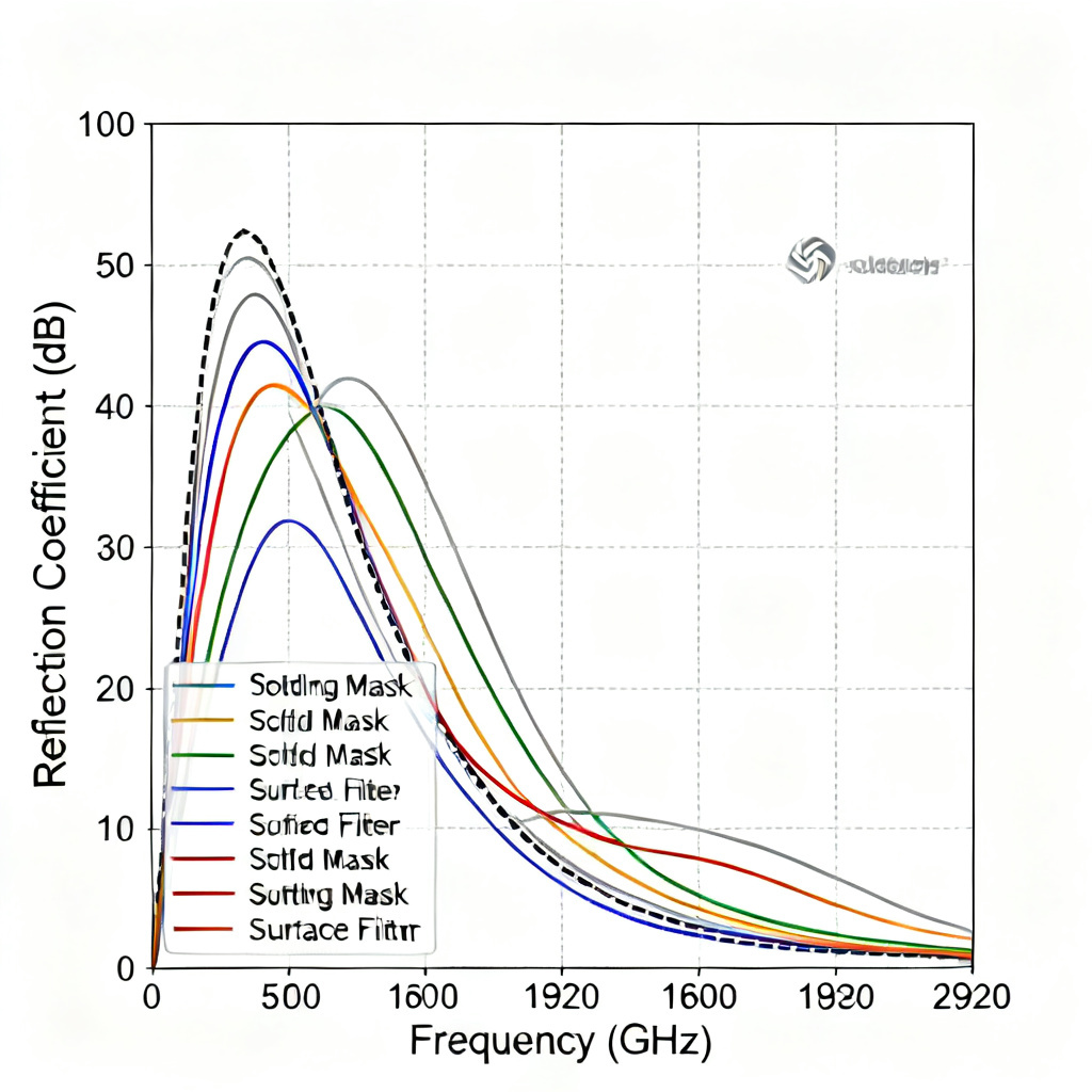
The reflection coefficient (Γ) for a discontinuity is Γ = (Zlocal – Z0) / (Zlocal + Z0). For a 50-ohm line, a 2-ohm impedance change due to solder mask yields Γ ≈ -0.02 (or -34 dB). This is a minor reflection but becomes significant with multiple discontinuities.
2.2 Frequency Domain Impact
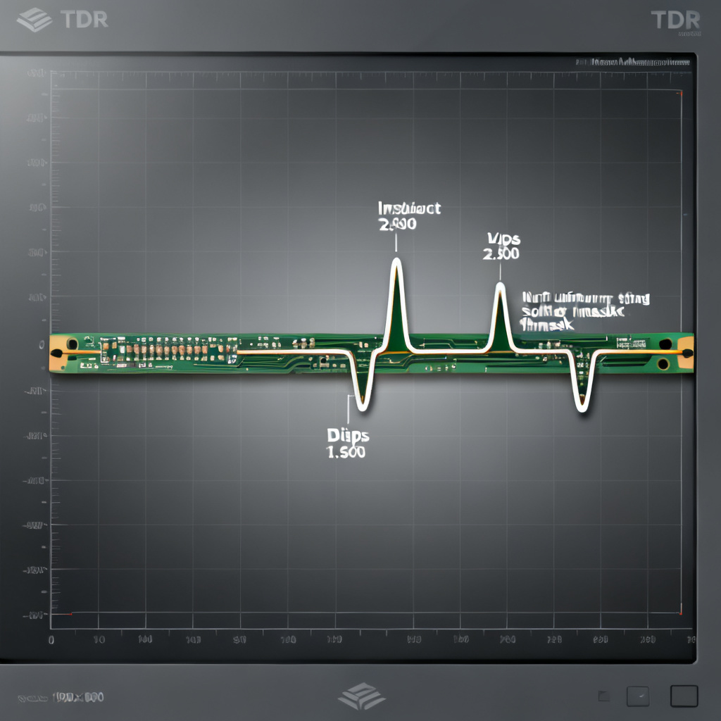
Using TDR analysis, a solder mask-induced impedance dip of 2 ohms over a 1-inch trace at 10 GHz creates ~0.5 ps of jitter. For differential pairs (e.g., USB 3.0, PCIe Gen 4), this can cause skew between P and N signals.
2.3 Practical Measurement Data
| Configuration | Impedance Shift (ohms) | Reflection Coefficient (dB) |
|---|---|---|
| Microstrip with solder mask | -1.5 to -3 | -34 to -40 |
| Stripline (inner layers, no mask) | 0 | N/A |
| ENIG surface finish | -0.5 to -1 | -40 to -46 |
| HASL surface finish | ±2 to ±4 | -28 to -34 |
Mitigation Strategies to Reduce How Solder Mask and Surface Finish Create Minor Reflections in Transmission Line
4.1 Solder Mask Design Rules
- Remove solder mask over critical traces for designs >5 GHz.
- Use low-εr solder mask (εr < 3.2, tan δ < 0.01).
- Control thickness within ±0.2 mils over the trace.
- Avoid covering differential pairs to prevent skew.
4.2 Surface Finish Selection
- For ≥10 Gbps: Use ENIG with thin nickel (3 µm max) and immersion gold (0.05 µm).
- For ≥20 GHz: Use Immersion Silver or OSP to minimize electrical impact.
- Avoid mixing finishes on same signal layer.
4.3 Impedance Modeling and Simulation
- Include solder mask in stackup using field solvers (e.g., Ansys Q3D, Polar Si8000).
- Model nickel layer as a thin resistor for ENIG finishes.
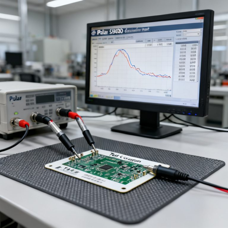
- Use TDR verification to measure impedance discontinuities post-fabrication.
4.4 Manufacturing Tolerances and Testing
- Set tight tolerances: solder mask thickness ±0.3 mils, surface finish thickness ±1 µm.
- Use coupon testing with and without solder mask to measure actual Z0 shift.
- Validate after thermal cycling (10 reflow cycles).
Frequently Asked Questions
How does solder mask create minor reflections in transmission line?
Solder mask alters the effective dielectric constant around the trace, lowering characteristic impedance by 1–5 ohms, which creates minor reflections in transmission line.
Which surface finish minimizes minor reflections in transmission line?
Immersion Silver and thin-nickel ENIG minimize minor reflections in transmission line due to their high conductivity and low impedance shift.
Can removing solder mask eliminate minor reflections in transmission line?
Yes, removing solder mask over critical high-speed traces eliminates the dielectric effect, reducing minor reflections in transmission line to near zero.
How do I measure minor reflections in transmission line caused by surface finish?
Use TDR (Time Domain Reflectometry) or VNA measurements to quantify impedance discontinuities caused by surface finish and solder mask.
What is the reflection coefficient for a typical solder mask-induced discontinuity?
For a 2-ohm impedance shift on a 50-ohm line, the reflection coefficient is approximately -34 dB, a minor reflection.
Comparison: Our High-Speed PCB Services vs. Standard Approaches
We specialize in high-speed PCB manufacturing with optimized solder mask and surface finish treatments. Unlike standard fabricators, we offer:
- Low-εr solder mask options (εr < 3.2) to minimize impedance shifts.
- Controlled surface finish thickness (ENIG nickel < 3 µm) for consistent impedance control.
- Free TDR impedance validation on all high-speed prototypes.
- Expert design support to remove solder mask over critical traces.
Glossary of Key Terms
- Characteristic Impedance (Z0): The constant impedance of a transmission line, typically 50 ohms or 100 ohms differential.
- Dielectric Constant (εr): A material property affecting signal propagation speed and impedance.
- Reflection Coefficient (Γ): The ratio of reflected voltage to incident voltage at a discontinuity.
- TDR (Time Domain Reflectometry): A measurement technique to locate impedance discontinuities.
- Skin Effect: The tendency of AC current to flow near the conductor surface at high frequencies.