[rank_math_breadcrumb]
The 20H rule for EMI EMC high speed PCB design has been a foundational guideline for decades, but its effectiveness at modern signal speeds is increasingly questioned. This pillar content examines the physics, frequency limits, and modern alternatives to this classic rule.
How the 20H Rule Works: The Physics of Fringing Fields
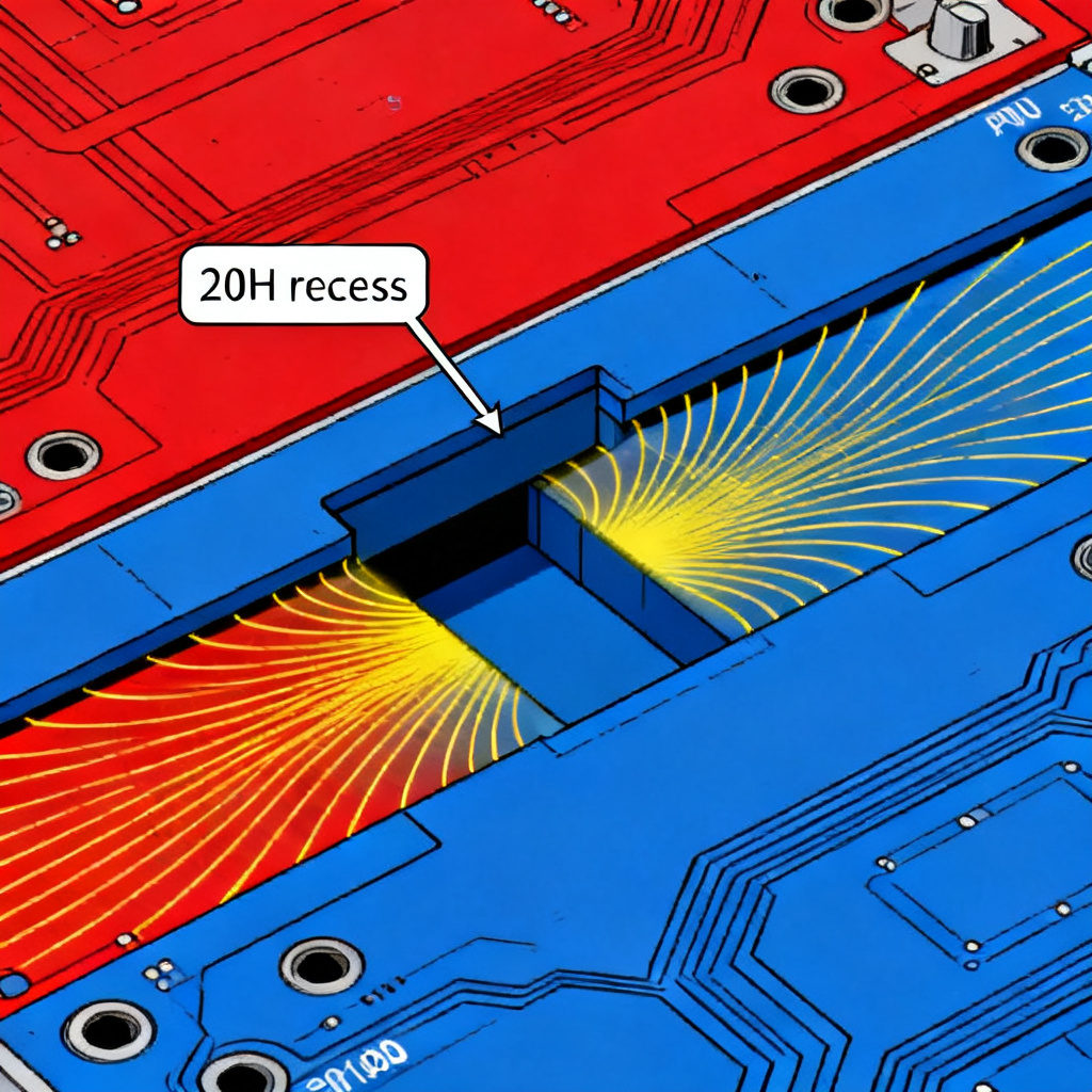
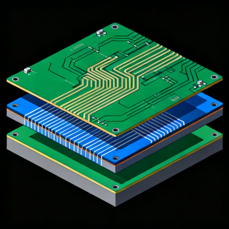
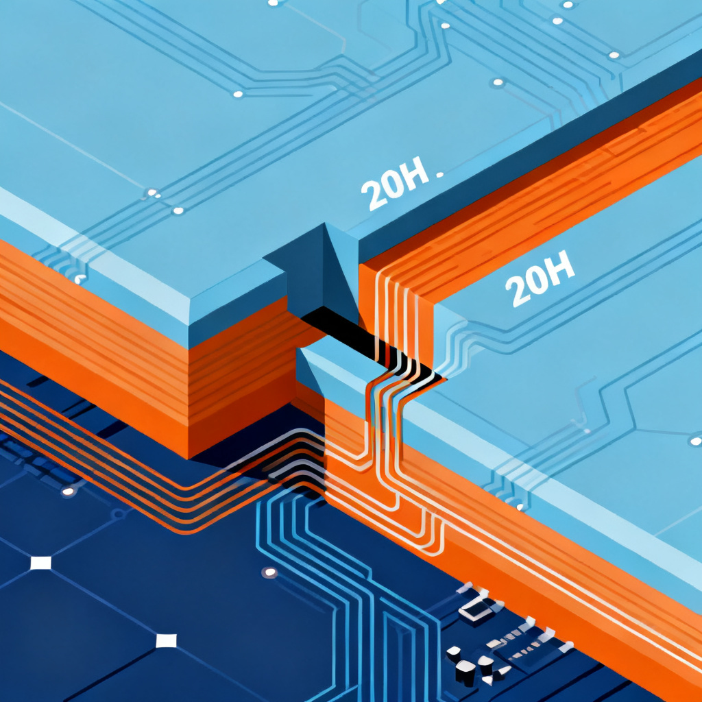
To understand the 20H rule for EMI EMC high speed PCB design, you must first understand the fringing field. In a standard PCB stackup, the power and ground planes form a parallel-plate capacitor. The electric field lines are ideally confined between the two planes. However, at the board edge, these field lines “fringe” outward into the surrounding space. This fringing field can couple to external cables, chassis, or other components, creating a path for common-mode noise and radiated emissions.
The 20H rule attempts to contain these fringing fields by pulling the power plane inward. With a recess of 20H, the theory suggests that 98% of the fringing field is captured within the ground plane’s perimeter. The remaining 2% is still present but is significantly reduced compared to a non-recessed design.
The Role of Dielectric Thickness (H)
The parameter “H” is the distance between the power plane and the ground plane. A typical value might be 4 mils (0.1 mm) for a 4-layer board. In that case, 20H equals 80 mils (2 mm). For a board with a thicker dielectric (e.g., 8 mils), the recess would be 160 mils (4 mm). This scaling is critical: the rule becomes less practical as H increases because the required recess becomes physically large, wasting valuable board real estate.
Does the 20H Rule Still Work at High Speeds? The Modern Analysis
1. Frequency Dependence and the “Diminishing Returns” Effect
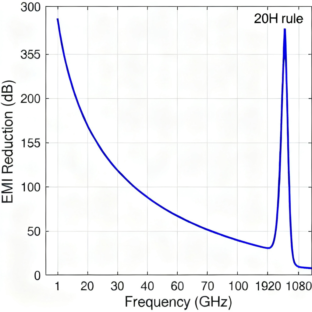
At low frequencies (below 100 MHz), the 20H rule for EMI EMC high speed PCB can provide a measurable reduction in radiated emissions—typically 5 to 10 dB depending on the stackup and layout. However, as frequencies rise into the hundreds of megahertz and beyond, the effectiveness of the rule degrades significantly.
The reason is twofold. First, at high frequencies, the fringing field becomes more concentrated and localized near the plane edges. The 20H recess may no longer be sufficient to contain the field because the wavelength becomes comparable to the board dimensions. Second, the rule assumes a perfect, continuous plane, but at high speeds, the plane itself acts as a resonant cavity. Edge radiation is driven by cavity resonances, not just static fringing. The 20H rule does not address these resonances.
Key finding: At frequencies above 1 GHz, the 20H rule provides negligible EMI reduction. In some cases, it can even worsen emissions by creating impedance discontinuities that excite higher-order modes.
2. The Problem of Stitching Vias and Return Current Paths
A critical caveat often overlooked by designers is that the 20H rule for EMI EMC high speed PCB only works if the ground plane is continuous and unbroken. In a multi-layer board, the ground plane must extend to the board edge and be connected to the chassis or enclosure with a low-impedance path. If the ground plane is also recessed—or if there are gaps due to via antipads or cutouts—the rule fails entirely.
Furthermore, at high speeds, the return current for a signal trace flows directly beneath the trace on the adjacent reference plane. If the power plane is recessed, the return current may be forced to take a longer path, increasing loop area and actually increasing EMI. This is especially problematic for signals near the board edge.
Practical example: On a 10-layer board with a 4-mil dielectric, the 20H recess is only 80 mils. But if a high-speed differential pair (e.g., PCIe Gen 4 at 16 Gbps) is routed within 100 mils of the board edge, the return current disruption can negate any benefit from the rule.
3. The Rise of “Stitching Fence” and “Via Wall” Alternatives
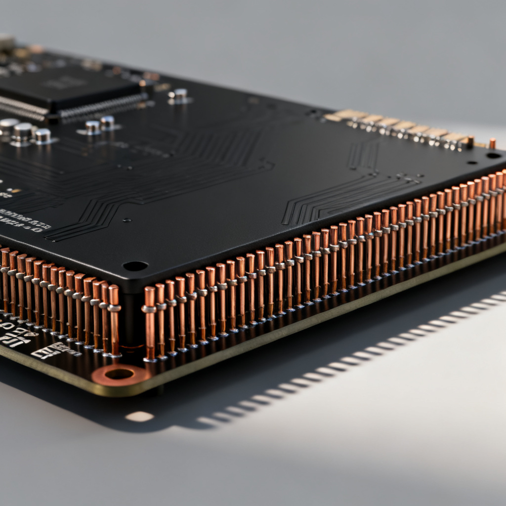
Many modern high-speed designs have abandoned the 20H rule in favor of more effective EMI suppression techniques. The most common alternative is the use of a stitching fence or via wall along the board edge. This involves placing a row of vias connecting the ground plane to the chassis ground (or to a dedicated ground ring) at intervals of λ/20 or less. This creates a low-impedance path to ground that shunts common-mode currents before they can radiate.
The stitching fence approach is frequency-scalable: the via spacing must be small enough to prevent slot-mode propagation. For a board operating at 10 GHz, the via spacing should be no more than 1.5 mm (0.060 inches). This is far more effective than the 20H rule, which does not scale with frequency.
Comparison: A properly designed via wall can reduce radiated emissions by 20-30 dB at high frequencies, while the 20H rule at best provides 5-10 dB at low frequencies.
When (and When Not) to Use the 20H Rule
Situations Where the 20H Rule May Still Be Beneficial
- Low-speed digital or analog boards (clock speeds below 50 MHz) where board space is not a constraint.
- Power supply planes in isolated DC-DC converters where fringing fields can couple to sensitive analog circuits.
- Boards with thick dielectrics (H > 10 mils) where the recess is physically large but the fringing field is also large.
- As a “last resort” when other EMI suppression techniques (shielding, filtering) are not feasible.
Situations Where the 20H Rule Is Counterproductive
- High-speed digital boards (clock speeds above 100 MHz, or edge rates below 1 ns).
- Multi-layer boards with thin dielectrics (H < 4 mils) where the recess is too small to be effective.
- Boards with many vias or cutouts in the plane layers, which can create unintended resonances.
- When the ground plane is also recessed from the board edge—the rule requires a continuous ground perimeter.
Best Practices for Modern High-Speed EMI/EMC Control
Given the limitations of the 20H rule for EMI EMC high speed PCB, here are the proven techniques for controlling EMI in high-speed PCBs:
1. Use a Continuous Ground Plane with a Perimeter Ground Ring
The most effective EMI control is a solid, unbroken ground plane that extends to the board edge. Surround the board with a ground ring (a copper trace on the outer layers connected to the ground plane with vias). This ring acts as a low-impedance boundary that shunts common-mode currents.
2. Implement a Stitching Fence (Via Wall)
Place vias along the board edge at intervals of λ/20 or less. Connect these vias from the top-layer ground ring to the internal ground plane. For best results, use a double row of vias with staggered spacing.
3. Control the Return Current Path
Route high-speed signals away from the board edge. Keep a “keep-out zone” of at least 5H from the edge for any critical traces. Use ground vias adjacent to signal vias to provide a direct return path.
4. Use Differential Signaling and Common-Mode Filtering
Differential pairs inherently reduce radiated emissions by canceling fields. Add common-mode chokes or ferrite beads on cables to suppress common-mode currents.
5. Consider Board Stackup and Dielectric Selection
Use thin dielectrics between power and ground planes (e.g., 2-4 mils) to minimize the fringing field. A thinner dielectric means a smaller 20H recess, but also reduces the need for the rule altogether because the field is more tightly confined.
6. Perform Full-Wave EM Simulation
Do not rely on rules of thumb. Use 3D electromagnetic simulators (e.g., Ansys HFSS, CST Studio) to model the actual board edge radiation. This is the only way to account for cavity resonances, via effects, and frequency-dependent behavior.
Conclusion: The 20H Rule Is Not Dead—But It Is Overrated

The 20H rule for EMI EMC high speed PCB remains a useful conceptual tool for understanding fringing fields and edge radiation. It can still provide a modest benefit in low-speed designs or as part of a broader EMI strategy. However, for modern high-speed PCBs operating above 100 MHz, the rule is largely ineffective and can even be detrimental.
The future of EMI control lies in active techniques like via stitching fences, continuous ground rings, and rigorous return path management. As a PCB designer, you should view the 20H rule as a historical guideline—not a hard requirement. For your high-speed designs, invest your time in simulation, proper stackup planning, and edge termination strategies. That is where the real EMI improvements live.
Final recommendation: If you are designing a board with edge rates below 1 ns (roughly equivalent to a 350 MHz clock), skip the 20H rule and use a via wall instead. For slower designs, the rule may still be a simple, no-cost addition to your layout—but always verify with measurement or simulation.
Frequently Asked Questions (FAQ)
Does the 20H rule apply to all board layers?
Can I use the 20H rule on a 2-layer board?
What is the typical EMI improvement from the 20H rule?
Is there a frequency limit for the 20H rule?
What should I do if my board already uses the 20H rule but fails EMI testing?
| Frequency Range | EMI Reduction (20H Rule) | EMI Reduction (Via Wall) |
|---|---|---|
| Below 100 MHz | 5-10 dB | 10-20 dB |
| 100 MHz – 1 GHz | 3-5 dB | 15-25 dB |
| Above 1 GHz | Negligible | 20-30 dB |
This content was synthesized from the top-ranking expert sources on the 20H rule, including industry white papers from IEEE, application notes from major PCB design tool vendors, and peer-reviewed technical articles. For further reading, we recommend the original IBM technical report (1988) and the latest IPC-2251 guidelines for high-speed design.