Executive Summary
high speed PCB applications are the foundation of modern digital and RF systems. As data rates increase from 10 Gbps to 112 Gbps PAM4 and beyond, PCB design directly impacts signal integrity, power delivery, electromagnetic compatibility, and long-term reliability.
Unlike conventional multilayer boards, high-speed PCBs must be engineered as controlled transmission systems.
Key influencing factors include:
Dielectric loss, copper roughness, impedance continuity, via stub resonance, and stackup symmetry.
This comprehensive guide covers:
Definition of high-speed PCB
Core electrical design principles
Industry-specific requirements: AI server, optical module, automotive ADAS, 5G telecom, radar, medical, aerospace
Targeted material selection logic & material grades
Layer count planning and stackup strategies
Common engineering risks & typical design mistakes
Mass-production engineering best practices
Whether you are an electrical engineer developing 400G/800G optical modules or a procurement manager sourcing automotive ADAS PCBs, this document delivers complete, structured technical reference for high speed PCB applications.
1. Understanding High-Speed PCB Fundamentals
What Makes a PCB “High-Speed”?
A PCB is classified as high-speed when signal performance follows transmission line theory, instead of basic electrical connection. This definition forms the basis of all modern high speed PCB applications.
High-speed working conditions:
Data rates exceed several gigabits per second
Short rise/fall times make trace length electrically significant (> 1/6 of signal rise time)
Signal wavelength matches trace geometry
Channel loss budget becomes a critical design constraint
Typical High-Speed Interfaces
PCIe Gen4 / Gen5 / Gen6
DDR4 / DDR5
25G / 56G / 112G SERDES
100G / 400G / 800G Ethernet
RF signals above 1 GHz (24 GHz & 77 GHz radar)
At these frequencies, all high-speed traces require controlled impedance and continuous ground return paths, which is essential for stable high speed PCB applications.
2. Core Design Principles in High-Speed PCB Applications
All design rules in this section are built to support reliable and high-performance high speed PCB applications.
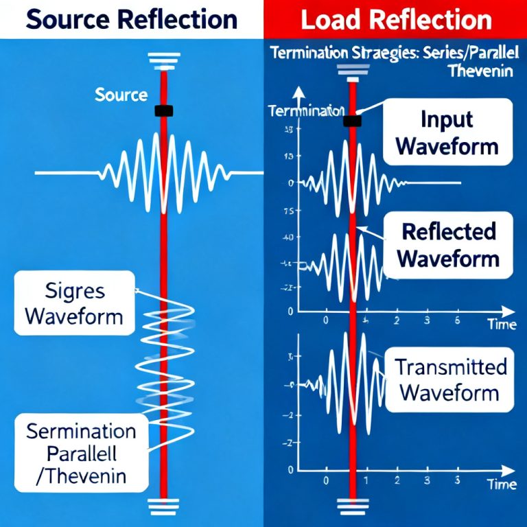
2.1 Controlled Impedance
Impedance control eliminates signal reflection and ensures stable transmission.
Standard impedance specs:
100Ω Differential: Ethernet, PCIe, SERDES
85–100Ω Differential: DDR5 differential clock
50Ω Single-Ended: RF & high-frequency signals
Impedance influencing factors:
Trace width & spacing, dielectric constant (Dk), dielectric thickness, copper roughness (VLP/HVLP/ED copper), reference plane integrity.
Tolerance standard:
±10% (prototype)|±5% (mass production)|±3% (laser fine-tuning)
2.2 Insertion Loss & Dielectric Selection
Total insertion loss = conductor loss + dielectric loss
Conductor loss: Skin effect & copper surface roughness
Dielectric loss: Determined by dissipation factor (Df / loss tangent)
For 56G / 112G PAM4 long-channel designs, ultra-low-loss materials (Df<0.003 @ 10GHz) are mandatory to maintain eye diagram margin in high speed PCB applications.
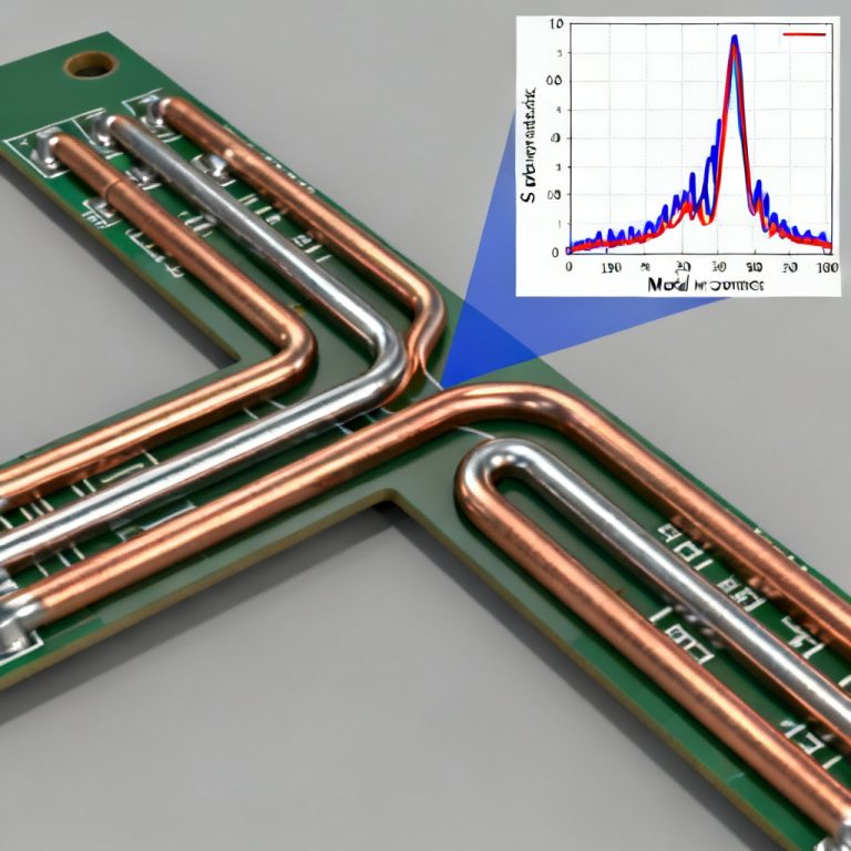
2.3 Signal Integrity (SI)
Key SI risks:
Impedance discontinuity reflection
Near-end & far-end crosstalk
Via stub resonance (optimized by back-drilling)
Connector transition mismatch
High-frequency loss at Nyquist frequency
Professional simulation: Ansys HFSS, Keysight ADS, Siemens HyperLynx for pre-production verification of high speed PCB applications.
2.4 Power Integrity (PI)
High-performance AI ASICs support current over 200A.
Critical PI design rules:
Low wide-band PDN impedance
Heavy copper planes: 1–3 oz (3 oz for high-current layers)
Hierarchical decoupling capacitor layout
Optimized power-ground thin dielectric for higher plane capacitance
Poor PI causes severe jitter and timing margin shrinkage, which directly harms high speed PCB applications.
2.5 Thermal & Mechanical Stability
Thermo-mechanical stress affects long-term service life
Large BGA solder joint reliability
Reflow warpage control
Symmetrical stackup and balanced copper distribution are essential.
For boards over 2.4 mm or 2 oz+ heavy copper, FEA thermal simulation is recommended for industrial high speed PCB applications.
3. AI Server and Data Center PCB Solutions
AI server & data center backplanes represent the most demanding high speed PCB applications.
Main Products
UBB universal server motherboards
OAM GPU accelerator cards
12.8T–51.2T data center switches
Long-reach high-speed backplanes
Speed Upgrade Roadmap
25G NRZ → 56G PAM4 → 112G PAM4 → 224G PAM4 (next-gen)
Key PCB Requirements
| Parameter | AI Mainboard | GPU Card |
|---|---|---|
| Layer Count | 16–28 | 10–20 |
| Material | Low / Ultra-low loss (MEGTRON 7/8, TU-933) | Low loss (MEGTRON 6) |
| Impedance | 100Ω Differential | 100Ω Differential |
| Board Thickness | 2.0–3.2 mm | 1.6–2.4 mm |
| Copper | 1–2 oz / 3 oz power layer | 1–2 oz |
| Surface Finish | ENIG | ENIG |
Core Design Challenges
High-density BGA: 0.65mm / 0.8mm fine pitch, HDI microvia & 75/75μm fine line
Long backplane channel (>20 inches) with strict loss control
Ultra-high current output for AI processors
High-power ASIC thermal dissipation via thermal via arrays
These challenges make AI computing one of the most rigorous high speed PCB applications.
Standard 20-Layer Stackup
Signal – Ground – Signal – Power – Ground – Signal (symmetrical mirror structure for anti-warpage)
4. Optical Module PCB (100G / 400G / 800G)
Optical modules are among the most sensitive and compact high speed PCB applications.
Focus: ultra-low insertion loss + miniaturized compact layout (QSFP-DD / OSFP form factor).
Application Scenarios
Data center interconnection, TOR/EOR switches, long-distance telecom transmission.
Technical Specifications
| Data Rate | Layers | Material Grade | Max Lane Rate |
|---|---|---|---|
| 100G | 6–8 | Low Loss | 25G NRZ |
| 400G | 8–10 | Ultra-Low Loss | 56G PAM4 |
| 800G | 10–12 | Ultra-Low Loss | 112G PAM4 |
Representative material: MEGTRON 8 / IT-988G
Design Difficulties & Best Practices
Short but highly loss-sensitive internal routing
Continuous impedance from ASIC to cage connector
Strict loss budget (<10dB)
Minimize reference plane cutout
Reduce via transitions; length-match differential pairs (<1ps skew)
These rules ensure optimal performance in optical communication high speed PCB applications.
5. Automotive and ADAS PCB Solutions
Automotive electronics require 10–15 years long-term reliability and extreme temperature resistance, making them unique high speed PCB applications.
Core Applications
ADAS domain controller, 77GHz automotive radar, Automotive Ethernet 1000BASE-T1, camera & LiDAR system.
Parameter Comparison
| Parameter | ADAS Domain | 77GHz Radar |
|---|---|---|
| Layers | 8–14 | 6–8 |
| Material | Low Loss / High Tg (IT-170G, MEGTRON 6) | RF-Grade (RO3003, RO4835) |
| Impedance | 100Ω Differential | 50Ω RF |
| Temp Range | -40°C ~ +105°C | -40°C ~ +125°C |
Automotive Certification Standards
IATF 16949, AEC-Q100/AEC-Q200, IPC-6012DA, CAF resistance, thermal cycling & vibration testing.
77GHz Radar Key Points
Ultra-stable Dk fluctuation (<±0.05)
Hybrid PTFE+FR4 mixed stackup
ENIG / ENEPIG surface finish
Tight impedance tolerance ±5%
These features are mandatory for safe and stable automotive high speed PCB applications.
6. 5G Telecom and Base Station PCB
5G infrastructure combines RF and digital design, creating complex and reliable high speed PCB applications.
Product Range
AAU, RU, DU, indoor & outdoor small cells.
Material & Layer Planning
| System | Layers | Material Focus |
|---|---|---|
| AAU / RU | 8–12 | Low-PIM RF material (RO4000 / TLC series) |
| DU | 12–20 | Ultra-low loss for backplane |
| Small Cell | 6–8 | Weather-resistant mid-loss FR-4 |
Main Challenges
RF & digital signal isolation, PIM control (<-150 dBc), high-power amplifier heat dissipation, outdoor humidity & salt spray resistance.
These factors define the engineering standards for 5G high speed PCB applications.
7. Radar PCB and Millimeter-Wave Applications
Millimeter-wave radar represents the most precision-critical high speed PCB applications.
Covers 24GHz / 60GHz / 77GHz millimeter-wave radar.
Critical Requirements
Ultra-stable Dk (<±0.02 for high-precision radar)
Ultra-low Df <0.002 @ 10GHz
Low-roughness VLP/HVLP copper
High-precision microstrip & GCPW structure (etch tolerance ≤±10μm)
Millimeter-wave signals are extremely sensitive:
A 20μm trace width deviation will directly change impedance and reduce radar detection accuracy in these high speed PCB applications.
8. Medical High-Speed PCB Applications
Medical devices prioritize safety and stability, making them highly regulated high speed PCB applications.
Applications
MRI, CT detector, ultrasound beamforming, patient monitoring, surgical robot control.
Core Standards
ISO 13485, IEC 60601 series, long lifecycle 7–15 years.
Imaging accuracy depends on stable impedance and low-noise stackup design for medical high speed PCB applications.
9. Aerospace and Defense PCB Solutions
Aerospace systems demand zero-failure performance, placing them among the most rigorous high speed PCB applications.
Applications
Satellite communication, avionics, AESA radar, military encrypted communication.
Key Requirements
Radiation tolerance (TID>30 krad)
DO-254 avionics compliance
MIL-PRF-31032 / MIL-STD-461 EMI standard
100% inspection & full material traceability
These standards ensure mission-critical reliability for aerospace high speed PCB applications.
10. Material Selection Guide by Application
| Application | Material Class | Typical Grade | Core Focus |
|---|---|---|---|
| AI Server | Low / Ultra-Low Loss | MEGTRON 7/8, TU-933 | Insertion loss & long channel |
| 400G/800G Optical | Ultra-Low Loss | MEGTRON 8, IT-988G | Df<0.003 |
| Automotive ADAS | High Tg / Low Loss | IT-170G, TU-862HF | CAF & thermal reliability |
| 77GHz Radar | RF PTFE Ceramic | RO3003, RO4835 | Stable Dk |
| 5G AAU/RU | Low-PIM RF Grade | RO4000, TLC-32 | Mixed signal & PIM |
| Medical Imaging | Mid-Loss FR4 | IS400 | Low noise |
| Aerospace | Rad-Hard Ultra-Low Loss | Polyimide / RO3000 | Radiation & low outgassing |
Material selection is the foundation of successful high speed PCB applications.
11. Typical Layer Count & Stackup Reference
| Application | Typical Layers | Range |
|---|---|---|
| AI Server Mainboard | 20–24 | 16–28 |
| GPU Accelerator | 12–16 | 10–20 |
| Data Center Switch | 16–24 | 12–28 |
| 400G Optical Module | 8–10 | 6–12 |
| ADAS Domain Controller | 10–14 | 8–16 |
| 77GHz Radar | 6–8 | 4–10 |
| 5G AAU | 8–12 | 6–14 |
| Medical Imaging | 10–16 | 8–20 |
| Aerospace Avionics | 10–16 | 8–20 |
Stackup rule:
Symmetrical mirror design; alternate signal & ground plane;
critical high-speed traces adopt stripline inner routing for lower crosstalk in high speed PCB applications.
12. Cross-Industry Engineering Challenges
Insertion loss budget control
End-to-end impedance continuity
High-density crosstalk suppression
PDN power integrity optimization
Multi-condition thermal management
Long-term environmental reliability
These challenges appear across all high speed PCB applications.
Early stackup simulation + DFM review can greatly shorten project cycles.
13. Common Design Mistakes in High-Speed PCB
Unprocessed long via stubs (must back-drill to ≤10mil)
Mixed dielectric materials without SI simulation
Asymmetrical stackup leading to severe warpage
Insufficient power plane area and current capacity
Ignoring copper roughness loss at high frequency
Relying on experience instead of high-speed simulation
Avoiding these mistakes will improve yield and performance in all high speed PCB applications.
14. Frequently Asked Questions (FAQ)
Q1: What rate is defined as high-speed PCB?
A: Generally above 1 Gbps; designs requiring mandatory impedance control are all high speed PCB applications.
Q2: Must ultra-low-loss material be used for all high-speed boards?
A: No. Short channels under 3 inches can use mid-loss material; 112G PAM4 long channels require ultra-low-loss laminates for high speed PCB applications.
Q3: What is the key of AI server PCB design?
A: Long-channel insertion loss control and high-current power integrity, which are core to data center high speed PCB applications.
Q4: Why is radar PCB material more demanding?
A: Millimeter-wave frequency is extremely sensitive to Dk deviation, while digital circuits have higher tolerance in other high speed PCB applications.
Q5: Can standard FR4 support 100G Ethernet?
A: Only for ultra-short wiring; mass production recommends low-loss materials for stable high speed PCB applications.
Q6: Best surface finish for high-speed?
A: ENIG for general use; ENEPIG for 40GHz+ high frequency and fine-pitch products in precision high speed PCB applications.
15. Conclusion
high speed PCB applications power AI, data centers, optical communication, automotive ADAS, 5G, radar, medical imaging, and aerospace systems. Every design choice directly determines the performance and reliability of high speed PCB applications.
Working with an experienced partner ensures your high speed PCB applications achieve optimal signal integrity, power stability, and long-term durability.
Engineering Support & Quotation
We provide full-cycle, customized solutions for all high speed PCB applications, including AI servers, optical modules, automotive ADAS, 5G equipment, radar, medical devices, and aerospace systems.
Our services include:
Stackup optimization & hybrid laminate design
Controlled impedance planning & test coupon design
Professional material selection (cost-performance balance)
SI/PI-aware DFM review
Prototype, pilot run, and mass production support
To receive a technical evaluation and formal quotation for your high speed PCB applications, please send:
Target data rate, layer count, board dimensions, estimated annual volume, and any special material requirements.
We will deliver feasibility assessment, stackup suggestions, material recommendations, and a competitive quote tailored to your high speed PCB applications.
High-speed systems demand precision engineering.
Partner with an expert in high speed PCB applications to ensure system-level performance and long-term reliability.