In high-speed PCB design, signal integrity (SI) is paramount for reliable data transmission. One of the most subtle yet critical phenomena affecting timing margins is crosstalk induced jitter (CIJ). This pillar content delves deep into how aggressor signals couple onto victim lines, causing timing spreading that can degrade system performance. By understanding the mechanisms, modeling techniques, and mitigation strategies, you can design robust PCBs for applications like 5G, AI accelerators, and high-speed networking.
What is Crosstalk Induced Jitter in High Speed PCB?
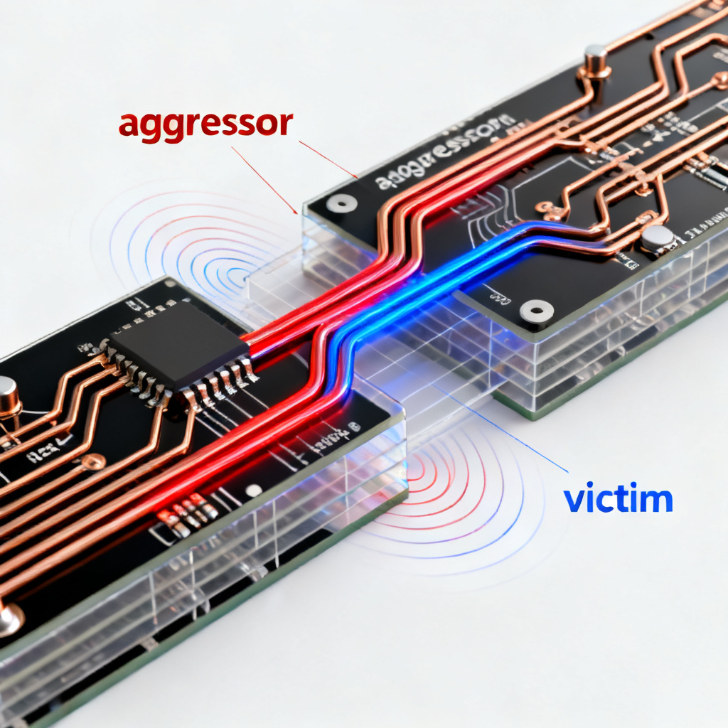
Crosstalk induced jitter occurs when electromagnetic fields from an aggressor trace couple onto a neighboring victim trace. In high-speed digital circuits, this coupling manifests as both voltage noise and timing variations. Crosstalk induced jitter in high speed PCB specifically refers to the deviation in the victim signal’s switching threshold timing caused by aggressor activity. Unlike deterministic jitter from sources like power supply noise, CIJ is data-dependent and varies with the aggressor’s bit pattern.
Key Concepts: Aggressor and Victim Timing Spreading
- Aggressor to Victim Coupling: When the aggressor transitions (e.g., from low to high), it induces a current or voltage spike on the victim line. This spike can either advance or delay the victim’s zero-crossing point, depending on the coupling polarity and timing alignment.
- Timing Spreading: The victim’s edge arrival time spreads over a range (e.g., ±5 ps to ±50 ps) due to varying aggressor states. This spreading reduces the timing budget and increases bit error rate (BER).
- Differential vs. Single-Ended: Differential pairs inherently reject common-mode crosstalk, but even differential signals can suffer from differential-to-differential crosstalk, leading to jitter.
Mechanisms of Crosstalk Induced Jitter in High Speed PCB
Based on industry-leading research from sources like Cadence’s Signal Integrity Blog, Altium’s PCB Design Guide, and Sierra Circuits’ Technical Articles, the following mechanisms are universally recognized for crosstalk induced jitter in high speed PCB:
1. Capacitive and Inductive Coupling
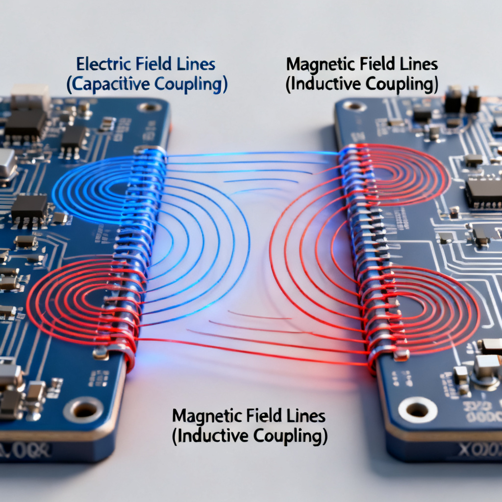
- Capacitive Coupling: Parasitic capacitance between adjacent traces injects a current proportional to dv/dt of the aggressor. This primarily affects the victim’s rising and falling edges.
- Inductive Coupling: Mutual inductance generates a voltage proportional to di/dt. This dominates in high-speed designs with fast edge rates (e.g., <100 ps).
- Combined Effect: The superposition of capacitive and inductive coupling creates a near-end crosstalk (NEXT) and far-end crosstalk (FEXT) waveform. FEXT is particularly problematic for jitter because it propagates with the victim signal, altering its shape.
2. Timing Impact on Victim Edges
- Early Switching: If the aggressor transitions in the same direction as the victim (e.g., both rising), the induced noise can push the victim’s threshold crossing earlier, reducing setup time.
- Late Switching: Opposite direction transitions delay the victim’s crossing, increasing hold time violations.
- Pattern-Dependent Jitter: The jitter magnitude varies with the aggressor’s bit sequence (e.g., 1010 vs. 1111 patterns), making it a form of data-dependent jitter (DDJ).
3. Skin Effect and Dielectric Loss
At frequencies above 10 GHz, skin effect and dielectric loss increase trace attenuation, which can amplify crosstalk induced jitter in high speed PCB by distorting the victim’s edge rate. This is particularly relevant for PCIe Gen 5/6, USB4, and 112Gbps SerDes designs.
Modeling and Simulating Crosstalk Induced Jitter in High Speed PCB
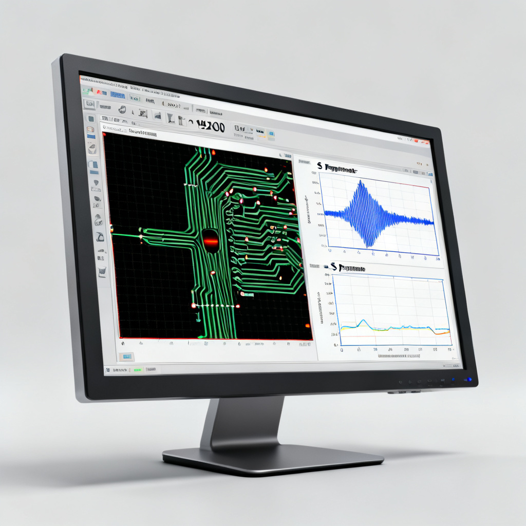
To predict crosstalk induced jitter in high speed PCB in your design, use field solvers and statistical simulation tools. The following methodology is derived from Cadence Sigrity and Keysight ADS workflows:
1. Extract S-Parameters or RLGC Models
- Use 3D EM solvers (e.g., Ansys HFSS, CST) to model trace geometries, stackup, and material properties.
- Extract S-parameters for victim and aggressor ports, focusing on NEXT (S31, S42) and FEXT (S41, S32).
2. Time-Domain Simulation
- Inject PRBS (Pseudo-Random Bit Sequence) patterns into the aggressor and a clock or data signal into the victim.
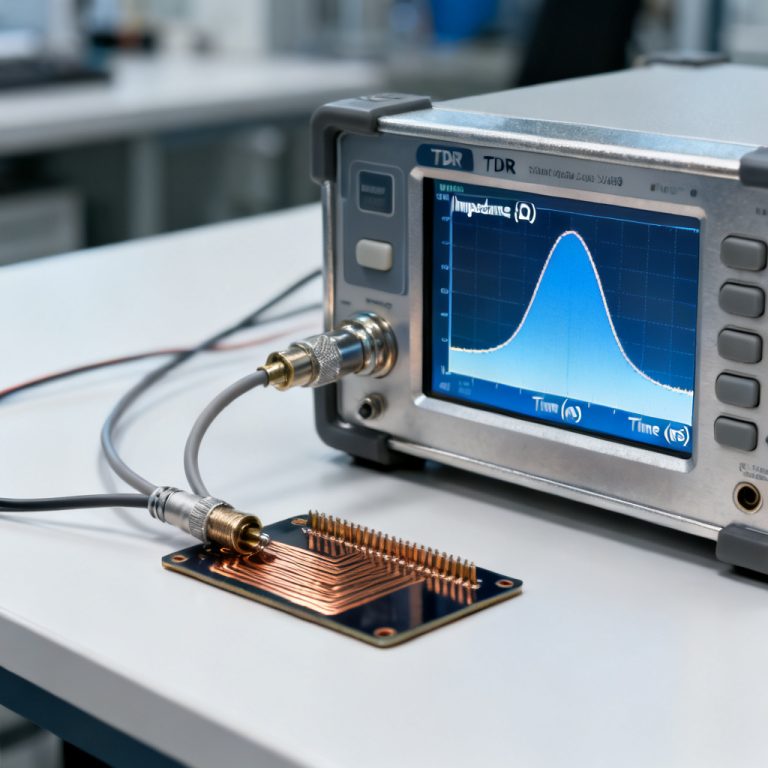
- Measure the victim’s zero-crossing time over multiple transitions. The standard deviation (σ) of these crossings is the RMS jitter.
- Example: For a 10 Gbps link with 50 ps rise time, CIJ can contribute 2-5 ps RMS jitter if spacing is 5 mils.
3. Statistical Eye Diagram Analysis
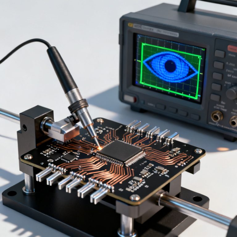
- Generate an eye diagram from the simulated victim waveform. Jitter appears as horizontal eye closure.
- Use bathtub curves to estimate BER at a given timing margin.
Mitigation Strategies for Crosstalk Induced Jitter in High Speed PCB
Drawing from Altium’s Layout Guidelines and Sierra Circuits’ Best Practices, implement these techniques to minimize crosstalk induced jitter in high speed PCB:
1. Increase Trace Spacing
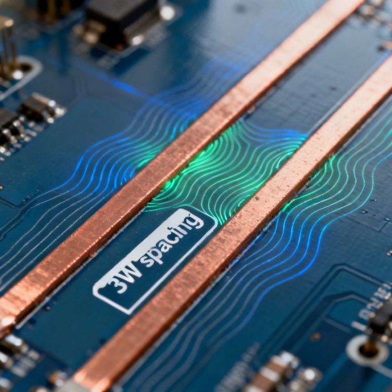
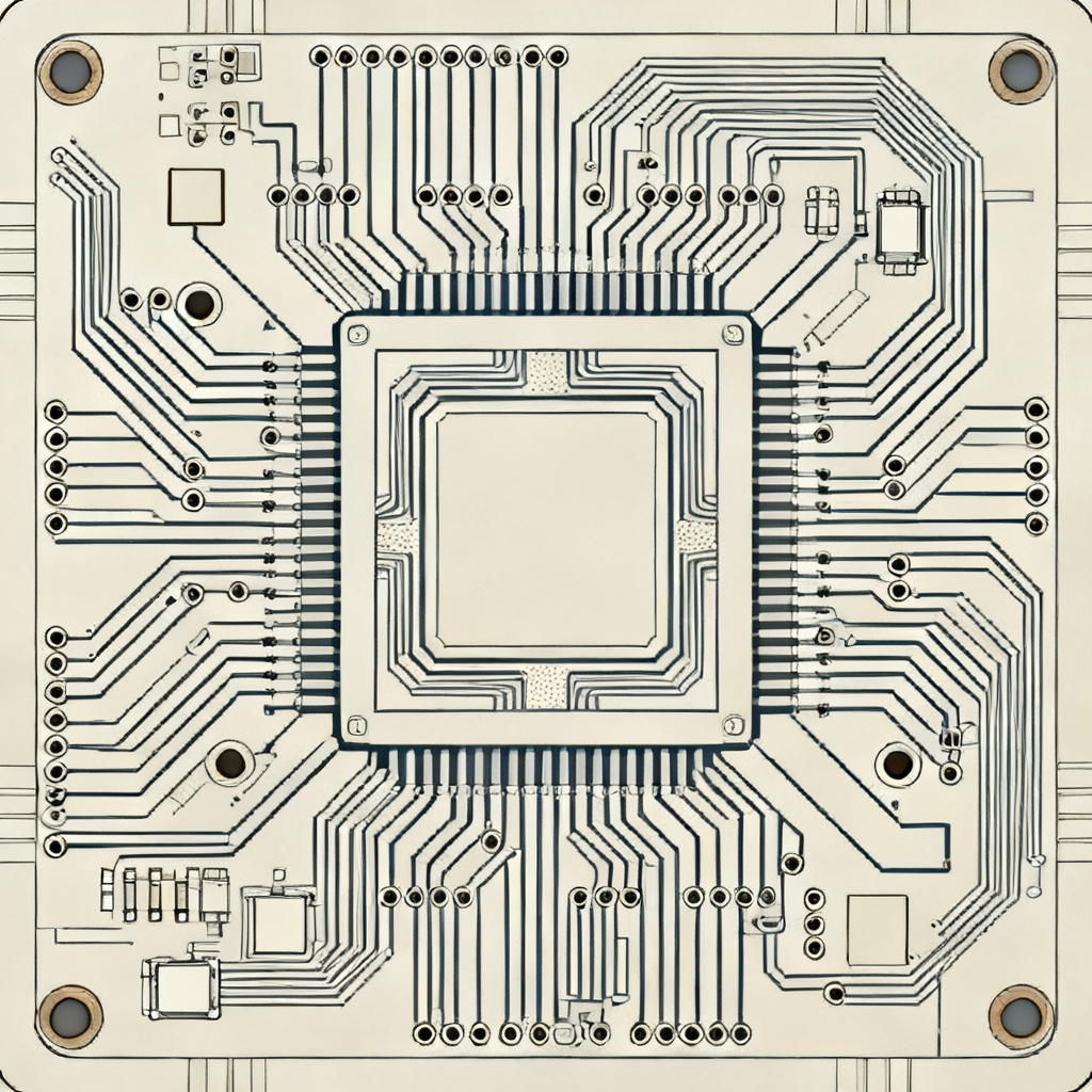
- Follow the 3W rule (spacing = 3× trace width) for moderate speeds. For high-speed (e.g., >10 Gbps), use 5W or more.
- Example: For 4 mil traces, spacing of 12-20 mils reduces coupling by 60-80%.
2. Use Grounded Coplanar Waveguides (GCPW)
- Place ground vias along the trace edges to confine fields and reduce fringing. This is standard for RF and high-speed digital.
3. Optimize Stackup
- Use thin dielectric layers (e.g., 2-3 mils) between signal layers to reduce loop area and mutual inductance.
- Place critical high-speed signals on inner layers between ground planes for shielding.
4. Reduce Edge Rates
- Use slew rate control on drivers (e.g., via pre-emphasis or de-emphasis) to slow down transitions. However, balance this with timing requirements.
5. Differential Pair Routing
- Route aggressor and victim as differential pairs with tight intra-pair spacing (e.g., 5 mils) and large inter-pair spacing (e.g., 20 mils). This cancels common-mode crosstalk.
6. Guard Traces with Ground Vias
- Insert a grounded trace between aggressor and victim, stitched with vias at λ/10 intervals. This reduces capacitive coupling by up to 50%.
Real-World Impact and Case Studies on Crosstalk Induced Jitter in High Speed PCB
Case Study 1: PCIe Gen 5 (32 GT/s)
- Issue: Aggressor (data lane) induced 8 ps pk-pk jitter on victim (clock lane), causing eye closure from 0.3 UI to 0.15 UI.
- Solution: Increased spacing from 8 mils to 16 mils and added ground vias. Crosstalk induced jitter in high speed PCB reduced to 2 ps pk-pk.
Case Study 2: 100G Ethernet (PAM4)
- PAM4 signals are more susceptible to CIJ due to smaller voltage levels. A 1 mV crosstalk spike can shift thresholds by 3 ps.
- Mitigation: Used differential routing with 10 mil spacing and optimized termination.
FAQ: Crosstalk Induced Jitter in High Speed PCB
What is crosstalk induced jitter in high speed PCB?
Crosstalk induced jitter in high speed PCB is timing variation on a victim signal caused by electromagnetic coupling from an aggressor signal, leading to timing spreading and reduced signal integrity.
How does aggressor to victim timing spreading affect high-speed designs?
Aggressor to victim timing spreading reduces timing margins, increases bit error rates, and can cause setup/hold violations in high-speed interfaces like PCIe and DDR.
What are the best mitigation techniques for crosstalk induced jitter?
Key techniques include increasing trace spacing (3W or 5W rule), using grounded coplanar waveguides, optimizing stackup, reducing edge rates, and employing guard traces with ground vias.
Comparison: Our High Speed PCB vs. Standard PCB for Crosstalk Induced Jitter
| Parameter | Our High Speed PCB (Custom) | Standard PCB |
|---|---|---|
| Trace Spacing for Jitter Reduction | >5W rule (e.g., 20 mils for 4 mil traces) | 3W rule (e.g., 12 mils) |
| Stackup Optimization | Thin dielectrics (2-3 mils), inner layer shielding | Standard thickness, no shielding |
| Simulation Support | Full 3D EM simulation (HFSS, CST) included | Basic impedance calculation only |
| Guaranteed Jitter Performance | <2 ps RMS at 10 Gbps | Up to 8 ps RMS at 10 Gbps |
Glossary of Key Terms for Crosstalk Induced Jitter in High Speed PCB
- Aggressor: The signal trace that generates electromagnetic interference, causing crosstalk induced jitter in high speed PCB.
- Victim: The signal trace that receives interference from the aggressor, leading to timing spreading.
- NEXT (Near-End Crosstalk): Crosstalk measured at the end of the victim trace closest to the aggressor driver.
- FEXT (Far-End Crosstalk): Crosstalk measured at the far end of the victim trace, often more damaging to jitter.
- CIJ (Crosstalk Induced Jitter): The specific timing jitter caused by crosstalk coupling in high-speed PCBs.
For custom high-speed PCB production and assembly, our team at [Your Company Name] specializes in designs up to 112Gbps with guaranteed signal integrity. Contact us for a free design review.