Duty Cycle Distortion in Eye Diagram PCB is a critical signal integrity issue that causes clock and data to drift apart, leading to bit errors in high-speed designs. This pillar page explains root causes, measurement techniques, and PCB design strategies to minimize Duty Cycle Distortion for reliable data transmission.
Understanding Duty Cycle Distortion in Eye Diagram PCB
What is Duty Cycle Distortion?
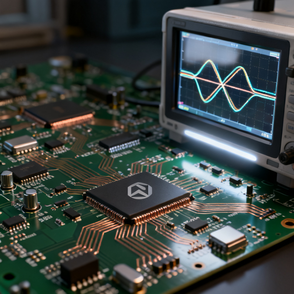
Duty Cycle Distortion in Eye Diagram PCB is a deterministic jitter component that manifests as a timing asymmetry in the signal. For a perfect clock signal with a 50% duty cycle, the high and low times are equal. DCD shifts this balance, causing the crossing point of the eye diagram to deviate vertically from its ideal position.
Key Characteristics:
- Pulse Width Imbalance: The high pulse is consistently longer or shorter than the low pulse.
- Deterministic Nature: Unlike random jitter, DCD is predictable and bounded, caused by specific phenomena in the transmitter, channel, or receiver.
- Frequency Dependence: DCD is often frequency-dependent; minimal DCD at lower speeds may become significant at target frequencies.
How DCD Appears in the Eye Diagram
When Duty Cycle Distortion in Eye Diagram PCB is present, the eye diagram loses its symmetrical appearance. The most telltale signs include:
- Vertical Eye Closure: The eye opening narrows vertically because threshold crossing points are no longer centered.
- Double-Line at the Crossing: Instead of a single crossing point, two distinct lines or a thickened band appear at the zero-amplitude level—the classic “dual-Dirac” signature of DCD.
- Asymmetric Eye Opening: The top half of the eye may appear wider or narrower than the bottom half, indicating a duty cycle imbalance.
Visualizing the Drift: A clock signal that is 55% high and 45% low causes rising and falling edges to misalign. Data-dependent jitter from DCD closes the eye on one side, shifting the optimal sampling point away from center.
Root Causes of Duty Cycle Distortion in Eye Diagram PCB
DCD stems from specific physical and design-related issues. We explore three primary categories of root causes.
Transmitter (TX) Induced DCD
The most common source of Duty Cycle Distortion in Eye Diagram PCB originates at the driver or serializer IC.
- Driver Asymmetry: Mismatched rise/fall times in the push-pull output stage (e.g., PMOS vs NMOS drive strength) translate directly into DCD.
- Clock Path Mismatch: Internal clock division or multiplication paths with mismatched delays introduce static duty cycle error.
- Data Pattern Dependence: Long identical bit strings (e.g., 1111) can shift DC bias, altering the duty cycle of the next transition.
Channel (PCB) Induced DCD
The PCB trace, connectors, and vias act as the transmission line; imperfections can exacerbate Duty Cycle Distortion in Eye Diagram PCB.
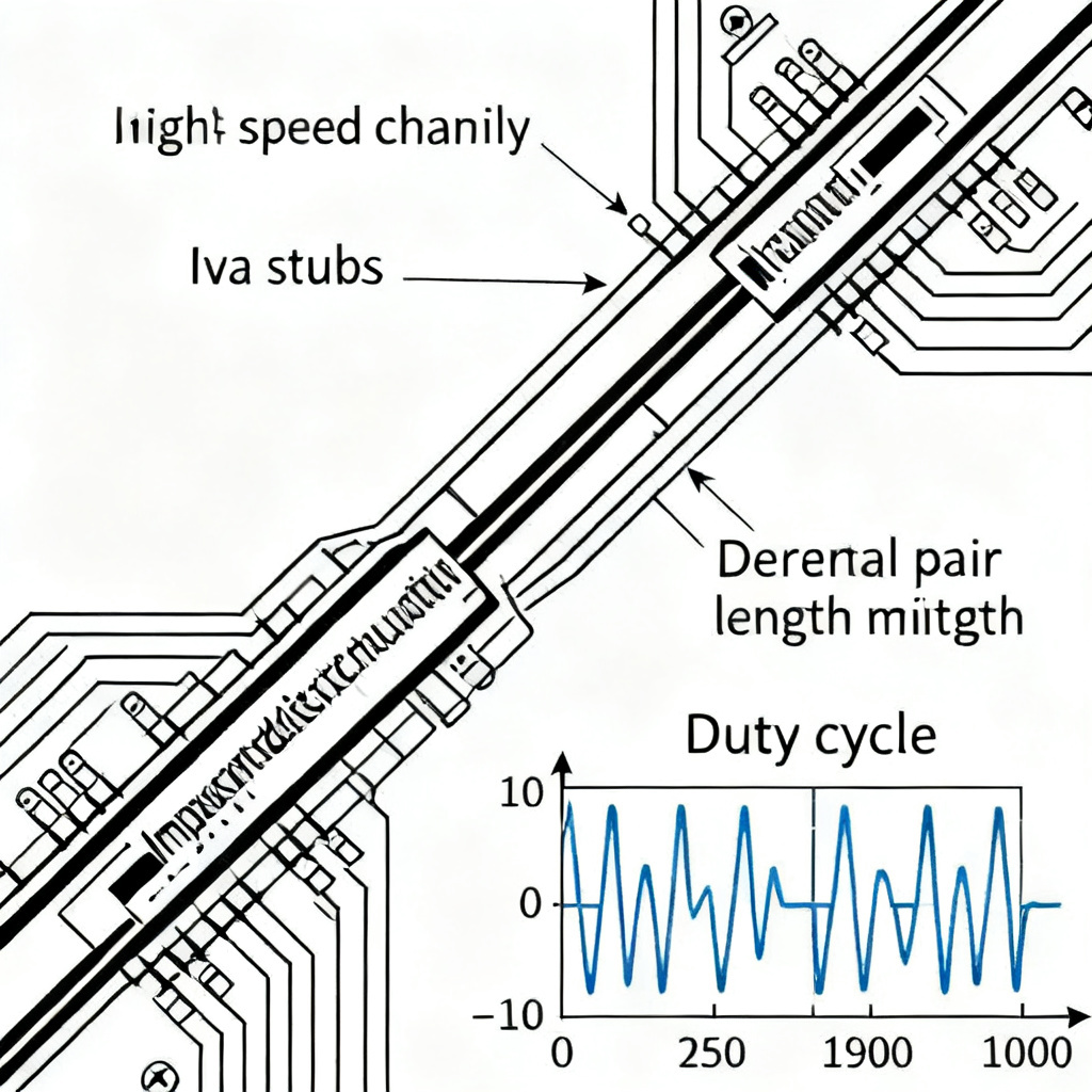
- Impedance Discontinuities: Reflections from mismatches (vias, connectors, stubs) add delayed signals that alter threshold crossing times.
- Skin Effect and Dielectric Loss: Frequency-dependent losses cause edge asymmetry—a slower rising vs falling edge is a form of DCD.
- Trace Length Mismatch in Differential Pairs: Skew between P and N traces shifts the differential crossing point, manifesting as DCD in the reconstructed signal.
Receiver (RX) Induced DCD
The receiver’s input stage can also contribute to Duty Cycle Distortion in Eye Diagram PCB.
- Threshold Offset: A comparator threshold not centered between ‘0’ and ‘1’ levels interprets a duty cycle error even if the transmitter is perfect.
- Input Capacitance Mismatch: Variations in differential pair input capacitance cause different delays for P and N signals, leading to differential skew and DCD.
Decomposing Jitter: Isolating DCD from Other Jitter Types
To effectively mitigate Duty Cycle Distortion in Eye Diagram PCB, one must first identify it through jitter decomposition.
The Dual-Dirac Model: This model describes deterministic jitter as having two distinct probability density functions—one for the left edge and one for the right edge of the eye. DCD appears as a separation between these two PDFs.
Measurement Techniques:
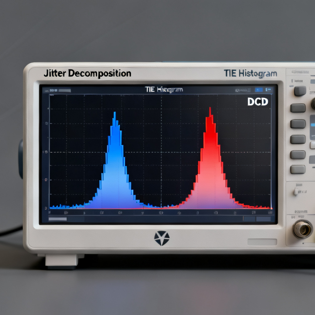
- Time Interval Error (TIE) Histogram: A bimodal distribution with two distinct peaks separated by the DCD magnitude.
- Bathtub Curve Analysis: DCD shifts the “floor” of the bathtub curve upward, reducing total jitter margin.
- Eye Diagram Mask Testing: DCD causes the signal to violate the mask more frequently on one side.
Key Distinction: DCD vs. ISI
- ISI is caused by channel memory effect (reflections, loss), creating a broad continuous jitter distribution.
- DCD is a static, pattern-independent offset at the crossing point, creating two distinct peaks in the histogram.
Quantifying and Modeling DCD
Mathematical Representation
Duty Cycle Distortion in Eye Diagram PCB is typically quantified as a percentage of the unit interval (UI) or as a time value.
- DCD (in UI): (T_high – T_low) / UI or (T_low – T_high) / UI
- DCD (in ps): |T_high – T_low|
For a 10 Gbps signal (UI = 100 ps), a DCD of 10% means a 10 ps difference between high and low pulse widths.
The DCD Jitter Component
The peak-to-peak jitter contributed by DCD (J_DCD) equals the magnitude of the duty cycle error. In the dual-Dirac model, this is the separation (δ) between the two Gaussian distributions.
Total Jitter (TJ) Approximation:
TJ = DJ + 14 * RJ (for BER = 1e-12)
Where DJ = DCD + ISI + PJ (Periodic Jitter)
Accurately measuring DCD allows you to subtract it from total DJ, clarifying other channel impairments.
PCB Design Strategies to Minimize DCD
This section covers essential techniques to minimize Duty Cycle Distortion in Eye Diagram PCB in your prototype-to-production runs.
Optimize the Transmitter Circuit
- Use Symmetrical Drivers: Choose ICs with low DCD specification (e.g., <5 ps) and matched rise/fall times.
- Pre-Emphasis/De-Emphasis: Tune carefully; over-equalization can introduce DCD via overshoot/undershoot.
- Clean Power Delivery: Provide stable, low-noise power supply to avoid amplitude modulation translating into DCD.
Master the PCB Channel
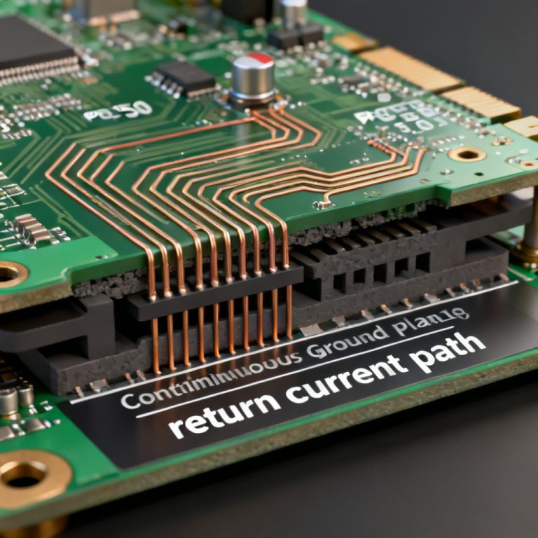
- Impedance Control: Maintain consistent characteristic impedance (e.g., 50Ω single-ended, 100Ω differential) with tight tolerances (±5% or better).
- Differential Pair Routing:
- Length Matching: Match P and N trace lengths within a few mils (<5 ps skew).
- Symmetry: Keep traces physically identical; avoid routing one over a ground plane cutout.
- Coupling: Maintain consistent spacing to control differential impedance.
- Minimize Vias: Use back-drilling to remove via stubs; use small, low-inductance vias when unavoidable.
- Material Selection: Use low-loss, low-DF materials (e.g., Megtron 6, Isola 370HR) to reduce dielectric absorption causing edge-rate asymmetry.
Receiver Design Considerations
- Use Adaptive Equalization: CTLE and DFE compensate for channel losses and reduce residual DCD impact.
- Adjust Sampling Threshold: Programmatically adjust decision threshold (V_th) to compensate for known static DCD.
Testing and Debugging DCD in Your PCB
Lab Measurement Setup
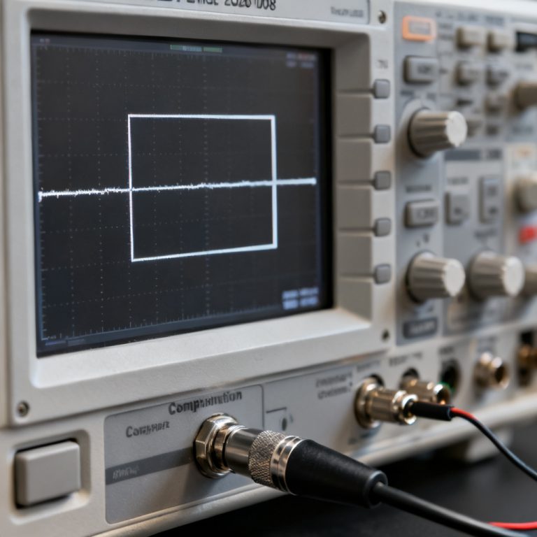
- Sampling Oscilloscope: Use high-bandwidth real-time or sampling oscilloscope (bandwidth 3-5x signal fundamental frequency).
- Differential Probe: Use low-capacitance, high-bandwidth differential probe.
- Clock Recovery: Use clock recovery module for data signals; direct trigger for clock signals.
Step-by-Step Debug Flow
- Visual Inspection: Look for classic double-line at the crossing in the eye diagram.
- Measure TIE Jitter: Use oscilloscope’s jitter analysis software; select “DCD” or “Deterministic Jitter” sub-menu.
- Compare Clock and Data: Measure clock signal directly; clean clock but distorted data indicates issue in data path or serializer.
- Vary Data Pattern: Use PRBS7 or PRBS31 pattern; compare with repeating “1010” pattern more sensitive to DCD.
- Temperature and Voltage Sweep: Sweep supply voltage and temperature to identify if DCD varies with PVT conditions.
Common Pitfalls in DCD Testing
- Trigger Jitter: Noisy trigger can mask DCD.
- Probe Loading: Probe capacitance can alter rise/fall times, introducing artificial DCD; use active probes.
- Pattern Generator Issues: Verify signal source first; it may itself have DCD.
Advanced Topics and Industry Implications
DCD in High-Speed SerDes
In modern SerDes (e.g., PCIe Gen 4/5, 100G Ethernet), Duty Cycle Distortion in Eye Diagram PCB is a critical specification. Transmitter DCD directly limits maximum achievable data rate over a given channel. Standards define strict DCD limits (e.g., <5% of UI) to ensure interoperability.
The Impact of DCD on Clock and Data Recovery (CDR)
The CDR circuit relies on data signal crossing points to extract a clock. DCD corrupts these crossing points, making it harder for the CDR to lock onto the correct phase. This causes the CDR to “drift” or “wander,” increasing jitter and bit errors—exactly when clock and data drift apart.
DCD and Signal Integrity (SI) Simulation
Before tape-out or fabrication, simulate high-speed links using tools like Ansys HFSS, Cadence Sigrity, or HyperLynx. These tools allow:
- Modeling the driver with realistic DCD specification.
- Simulating channel loss and reflections.
- Predicting eye diagram and jitter at the receiver.
- Key Parameter: Most SI tools allow input of “Duty Cycle Distortion” for the source; typical high-quality driver value is 2-5 ps.
Technical Terminology Explained
To deepen understanding of Duty Cycle Distortion in Eye Diagram PCB, here are key terms:
- Deterministic Jitter: Predictable, bounded jitter caused by specific phenomena like DCD or ISI.
- Dual-Dirac Model: A model describing deterministic jitter as two distinct probability distributions.
- Skin Effect: Frequency-dependent conductor resistance increase that rounds signal edges.
- Dielectric Loss (tan δ): Signal amplitude loss due to material properties, causing edge asymmetry.
- Back-Drilling: Removing unused via stubs to reduce impedance discontinuities.
DCD Specifications Table
| Duty Cycle Distortion Parameter | Value / Description |
|---|---|
| DCD in UI | (T_high – T_low) / UI |
| DCD in ps | |T_high – T_low| |
| Typical DCD limit (standards) | <5% of UI |
| High-quality driver DCD | 2-5 ps |
Comparison: DCD vs ISI in High-Speed PCB
| Aspect | Duty Cycle Distortion (DCD) | Inter-Symbol Interference (ISI) |
|---|---|---|
| Nature | Deterministic, static offset | Deterministic, pattern-dependent |
| Root Cause | Driver asymmetry, channel mismatch | Channel memory effect (reflections, loss) |
| Histogram Signature | Two distinct peaks | Broad, continuous distribution |
| Mitigation | Symmetrical routing, impedance control | Equalization, impedance matching |