In high-speed PCB design, jitter is the primary barrier to reliable data transmission. How equalization (CTLE/DFE/FFE) compensates jitter in high speed PCB is the critical knowledge for any engineer designing 10+ Gbps links. This pillar page explains the three dominant equalization techniques—CTLE, DFE, and FFE—and how they actively combat jitter to restore signal integrity. By understanding these methods, you can ensure your PCB designs achieve the lowest bit error rate (BER) and maximum channel reach.
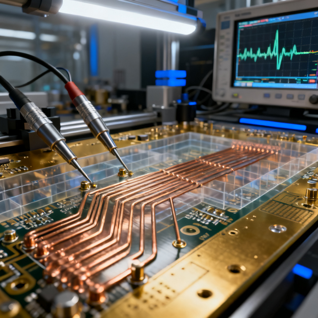
1. Understanding Jitter: The Root Cause
Before diving into the cures, we must understand the disease. Jitter is broadly categorized into two main types:
- Random Jitter (RJ): Unbounded, Gaussian in nature, caused by thermal noise, shot noise, and flicker noise. It cannot be predicted or eliminated, only tolerated.
- Deterministic Jitter (DJ): Bounded and predictable. It is further subdivided into:
- Data-Dependent Jitter (DDJ) / Inter-Symbol Interference (ISI): This is the most critical jitter type for equalization. ISI occurs when the channel’s frequency-dependent loss (skin effect and dielectric loss) causes a bit to “smear” into adjacent bits. A long string of 1s charges the channel capacitance, and then a single 0 looks like a weak 1. This creates a pattern-dependent timing shift.
- Duty Cycle Distortion (DCD): Caused by an asymmetric clock or threshold offset.
- Periodic Jitter (PJ): Caused by external noise coupling, power supply ripple, or switching noise.
The core problem: The channel acts as a low-pass filter. High-frequency components of the signal are attenuated more than low-frequency components. This distorts the signal’s shape, causing zero-crossing points to shift based on the previous data pattern. Equalization aims to undo this filtering effect.
2. Continuous Time Linear Equalization (CTLE) for Jitter Compensation
How equalization (CTLE/DFE/FFE) compensates jitter in high speed PCB begins with CTLE. CTLE is the first stage of equalization, typically implemented as an analog filter at the receiver (Rx) input. It is a linear, continuous-time circuit that amplifies high-frequency signal components more than low-frequency ones.
How CTLE Works
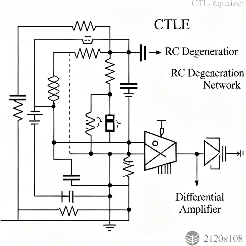
CTLE is essentially a high-pass filter with a controlled peaking gain. It uses a differential amplifier with a source-degeneration network (a resistor-capacitor (RC) pair). At low frequencies, the capacitor acts as an open, and the degeneration resistor reduces gain. At high frequencies, the capacitor shorts the resistor, increasing gain.
The key parameters of a CTLE are:
- DC Gain: The gain at low frequencies (typically 0 dB or slightly negative).
- Peaking Gain: The maximum gain at the peaking frequency (typically 6–12 dB).
- Peaking Frequency: The frequency at which the gain boost is maximum (often set near the Nyquist frequency of the data rate).
- Zero and Pole: The CTLE introduces a zero (at frequency f_z = 1/(2π*R_s*C_s)) and a pole (at f_p = f_z * (1 + g_m*R_s/2)), where R_s and C_s are the degeneration components.
How CTLE Compensates Jitter
CTLE directly targets DDJ/ISI caused by channel loss. By boosting the high-frequency energy of the incoming signal, CTLE restores the sharp edges of the data transitions. A sharper edge has a faster slew rate, meaning the signal crosses the receiver’s threshold at a more consistent time, regardless of the preceding bit pattern.
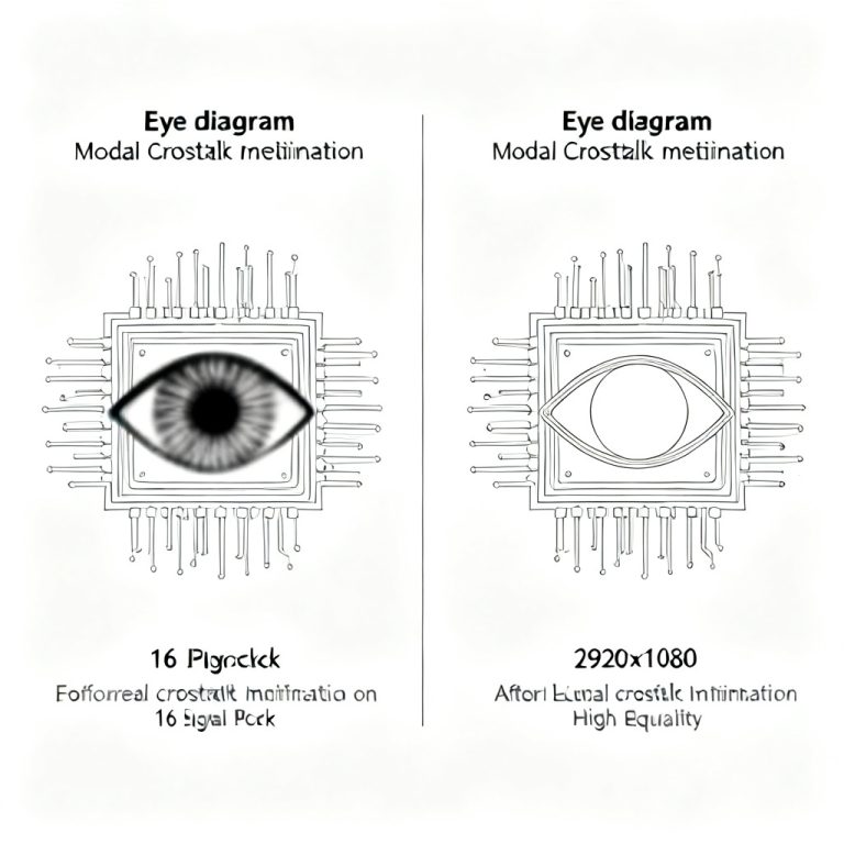
- Effect on Eye Diagram: CTLE opens the vertical eye opening (voltage margin) significantly. It also reduces the horizontal eye closure (time margin) by making the zero-crossing point more deterministic.
- Limitations: CTLE is a linear filter. It amplifies both the signal and the high-frequency noise (including crosstalk). If the channel loss is very high, the CTLE gain must be very high, which amplifies noise to unacceptable levels. This is the “noise enhancement” problem. Furthermore, CTLE cannot perfectly equalize a channel with a non-linear or complex frequency response. It is a “one-size-fits-most” filter.
CTLE in Practice
Modern SerDes designs (e.g., PCIe Gen 4/5, USB 3.2, 10G-KR) use adaptive CTLEs. The receiver automatically adjusts the peaking gain and peaking frequency based on the incoming signal’s quality, often by monitoring the signal amplitude at the slicer input or by using a built-in eye monitor.
3. Feed-Forward Equalization (FFE) for Jitter Mitigation
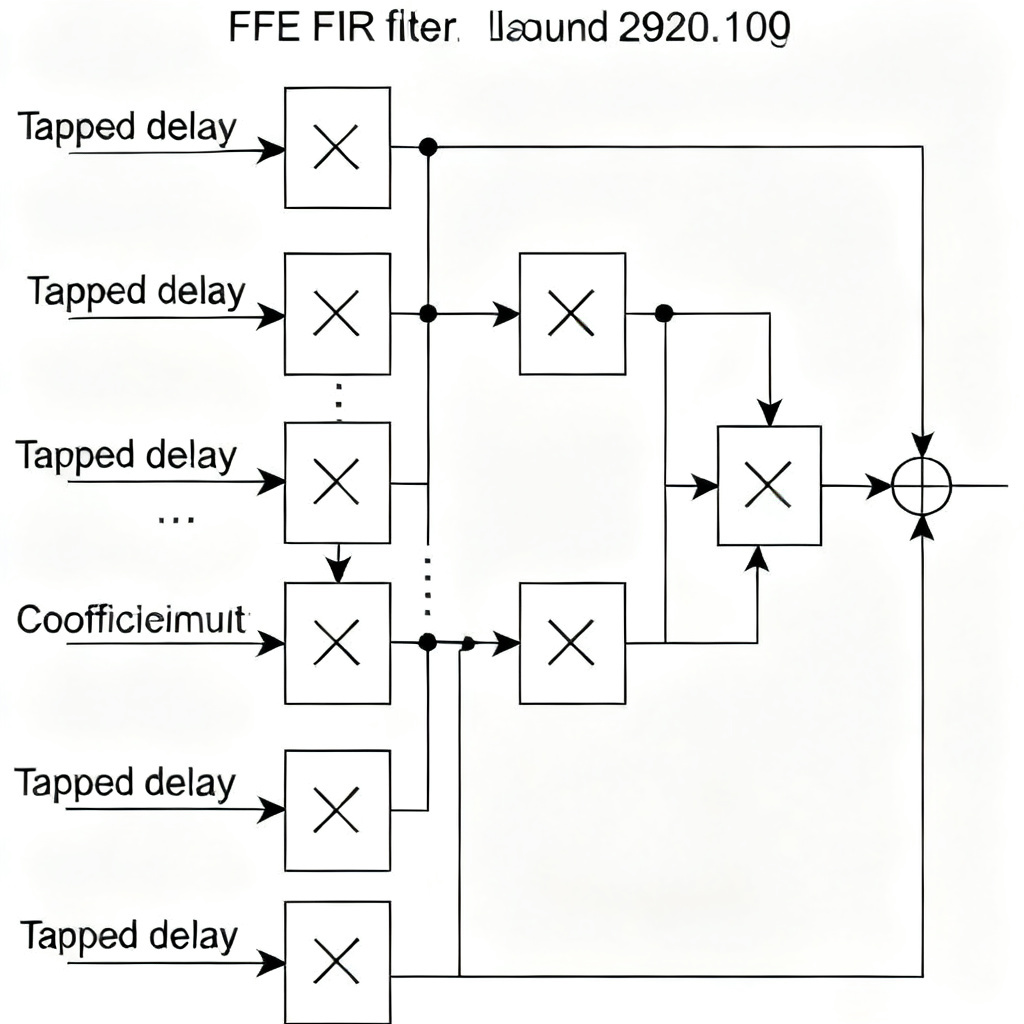
How equalization (CTLE/DFE/FFE) compensates jitter in high speed PCB also involves FFE at the transmitter. FFE, also known as a transmit equalizer (TxEQ) or pre-emphasis/de-emphasis, is implemented at the transmitter (Tx). It is a linear, discrete-time filter that pre-distorts the transmitted signal to compensate for the channel’s expected loss.
How FFE Works
FFE is a finite impulse response (FIR) filter. It consists of a tapped delay line with programmable tap coefficients. The output is a weighted sum of the current bit and several previous bits.
The typical implementation for a differential high-speed output is:
- Main Tap (C0): The current bit.
- Pre-Cursor Tap (C-1): The next bit (looks ahead).
- Post-Cursor Taps (C1, C2, …): The previous bits.
By adjusting the tap coefficients, the transmitter can:
- De-emphasis: Reduce the amplitude of the main tap (C0) relative to the pre- and post-cursor taps. This is the most common method for backplane channels.
- Pre-emphasis: Increase the amplitude of the pre- and post-cursor taps relative to the main tap.
The output voltage is: V_out = C-1 * D(t+T) + C0 * D(t) + C1 * D(t-T) + C2 * D(t-2T) + …
How FFE Compensates Jitter
FFE attacks the root cause of DDJ at the source. By pre-distorting the signal, it creates a waveform that, after passing through the lossy channel, will look like an ideal, clean signal at the receiver.
- Effect on Eye Diagram: FFE primarily improves the horizontal eye opening. It reduces the timing jitter caused by ISI. Because the signal is pre-distorted, the receiver sees a cleaner waveform with less need for high-frequency gain, thus avoiding the noise enhancement problem of CTLE.
- Limitations: FFE requires knowledge of the channel’s impulse response. The tap coefficients must be set correctly. If the channel changes (e.g., due to temperature or connector wear), the FFE may become suboptimal. FFE also consumes power in the transmitter, and the pre-distorted signal can have increased peak-to-average power ratio, potentially causing non-linearities in the output driver.
FFE in Practice
FFE is a standard feature in nearly all high-speed serial links. In PCIe Gen 3 and above, the transmitter has a 3-tap FFE (pre-cursor, main, post-cursor). In 100G Ethernet (CAUI-4), more complex FFE structures with 5 or more taps are common. The coefficients are typically set during a link training sequence, where the receiver sends back information about the channel quality.
4. Decision Feedback Equalization (DFE) for Jitter Cancellation
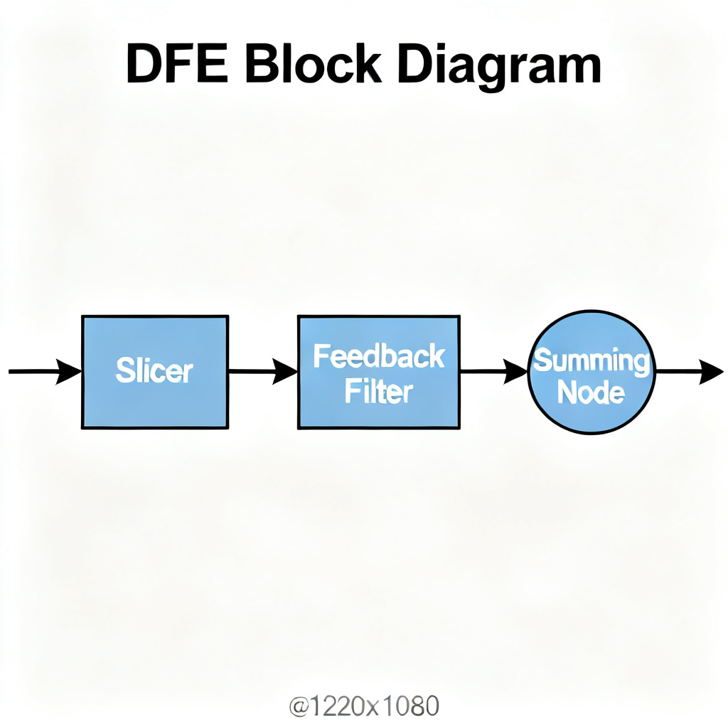
How equalization (CTLE/DFE/FFE) compensates jitter in high speed PCB reaches its most powerful form with DFE. DFE is a non-linear, discrete-time filter implemented at the receiver (Rx). Unlike CTLE and FFE, DFE does not amplify noise. It uses the decisions made by the receiver’s slicer (the circuit that determines if a bit is a 0 or a 1) to cancel the ISI caused by previous bits.
How DFE Works
A DFE consists of:
- Slicer (Decision Device): A comparator that samples the incoming signal and decides whether it is a 1 or a 0.
- Feedback Filter: A tapped delay line that stores the previous decisions (not the analog signal).
- Summing Node: The output of the feedback filter is subtracted from the incoming signal before the slicer.
The DFE works on the principle that the ISI caused by a previous bit is predictable. If the receiver knows the value of the previous bit (e.g., bit N-1 was a 1), it can subtract the expected ISI contribution of that bit from the current bit (bit N). This is done using a feedback tap coefficient (h1). For a 1-tap DFE, the operation is: V_in_compensated = V_in – h1 * D(N-1).
How DFE Compensates Jitter
DFE is extremely effective at canceling post-cursor ISI—the interference from bits that came before the current bit. This is the dominant form of ISI in most channels.
- Effect on Eye Diagram: DFE dramatically opens the horizontal eye opening. It removes the “long tail” of the channel’s impulse response. Because the feedback is based on clean digital decisions (0 or 1), there is no noise enhancement. This allows DFE to handle channels with very high loss that would be impossible for CTLE alone.
- Limitations:
- Error Propagation: If the slicer makes an incorrect decision (a bit error), the DFE will subtract the wrong ISI value, potentially causing the next bits to also be incorrect. This leads to a burst of errors.
- Pre-cursor ISI: DFE cannot cancel pre-cursor ISI (interference from future bits). This must be handled by FFE.
- Complexity: DFE requires a timing recovery circuit that is synchronized with the data rate. The feedback loop must settle within one unit interval (UI), which becomes extremely challenging at very high data rates (e.g., > 56 Gbps). This limits the number of DFE taps that can be practically implemented.
DFE in Practice
DFE is the workhorse of modern high-speed receivers. PCIe Gen 3/4/5 uses a DFE with up to 4 taps. 25G Ethernet (KR) and 100G Ethernet use DFE with 5–15 taps. The DFE taps are adaptively trained during link initialization, often using a Least Mean Squares (LMS) algorithm.
5. The Combined Equalization Architecture: CTLE + FFE + DFE
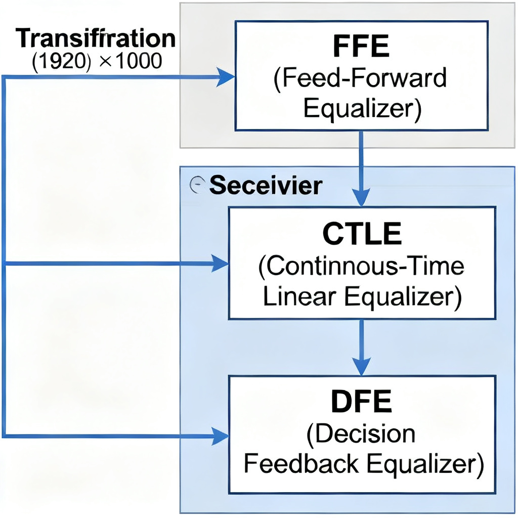
No single equalizer is perfect. The optimal solution for a high-speed PCB link is a hybrid architecture that combines all three techniques. The typical signal path in a modern SerDes is:
- Transmitter (Tx): FFE pre-distorts the signal to cancel pre-cursor ISI and a portion of post-cursor ISI. This reduces the burden on the receiver.
- Channel: The signal travels through the lossy PCB trace, connector, and cable.
- Receiver (Rx):
- CTLE: The first stage. It provides a fixed or adaptive high-frequency boost to open the vertical eye and reduce the amplitude of the post-cursor ISI tail.
- DFE: The second stage. It takes the CTLE output, samples it, and subtracts the remaining post-cursor ISI based on the decisions. This is the final, most precise cancellation step.
Why this combination works:
- FFE handles pre-cursor ISI and reduces the overall ISI magnitude.
- CTLE provides a linear boost to overcome the channel’s low-pass filter effect, making the signal large enough for the DFE slicer.
- DFE cancels the residual post-cursor ISI without noise enhancement, achieving the lowest possible BER.
| Technique | Location | Type | Jitter Type Compensated | Noise Enhancement | Typical Application |
|---|---|---|---|---|---|
| CTLE | Receiver | Linear, continuous | DDJ/ISI (high-frequency boost) | Yes | PCIe Gen 4/5, USB 3.2 |
| FFE | Transmitter | Linear, discrete | Pre-cursor & post-cursor ISI | No (pre-distortion) | PCIe Gen 3+, 100G Ethernet |
| DFE | Receiver | Non-linear, discrete | Post-cursor ISI | No | PCIe Gen 3/4/5, 25G/100G Ethernet |
6. Practical Implications for High-Speed PCB Design
As a B2B PCB manufacturer, understanding these equalization techniques allows you to advise your clients on design trade-offs. How equalization (CTLE/DFE/FFE) compensates jitter in high speed PCB directly influences material selection, stackup, and routing rules.
- Channel Loss Budget: The total equalization capability of the SerDes must match the channel loss. A channel with 20 dB of loss at Nyquist might be handled by CTLE alone. A channel with 35 dB of loss requires a DFE. A channel with 45 dB of loss requires FFE + CTLE + DFE.
- PCB Material: For channels requiring high DFE gain, the PCB material must be consistent. DFE relies on the assumption that the channel’s impulse response is time-invariant. Lossy materials like FR-4 at high frequencies create non-linearities that degrade DFE performance. Low-loss materials (e.g., Megtron 6, Rogers 4350B) are essential for links relying on DFE.
- Stackup and Routing: Even with the best equalization, a poorly designed PCB will fail. Ensure:
- Controlled impedance (e.g., 100Ω differential ±10%).
- Minimal via stubs (use back-drilling or blind vias).
- Length matching within tight tolerances (e.g., ±5 mils for 25 Gbps).
- Avoidance of sharp 90-degree corners.
- Simulation: For any design above 10 Gbps, your client must perform channel simulation using IBIS-AMI models. These models include the SerDes equalization settings. You, as the PCB manufacturer, should provide accurate S-parameter models of your stackup and via structures to enable this simulation.
- Testing: A real eye diagram at the receiver’s input, after the CTLE but before the DFE, is a valuable diagnostic tool. If the eye is completely closed (no opening), the DFE may still be able to recover the data, but the link margin is very low. A clean, open eye at the receiver pad is the ultimate goal.
Our Advantage: We specialize in fabricating PCBs optimized for high-speed equalization. Our controlled impedance tolerances are within ±5%, and we provide full S-parameter data for your simulation models. This ensures that your CTLE, DFE, and FFE settings work as intended, minimizing jitter and maximizing link margin.
Frequently Asked Questions
What is jitter in high-speed PCB design?
Jitter is the deviation of a signal’s timing from its ideal position. In high-speed PCB design, jitter is primarily caused by inter-symbol interference (ISI) due to channel loss, and it directly impacts the bit error rate (BER) of the link.
How does CTLE compensate jitter in high speed PCB?
CTLE (Continuous Time Linear Equalization) compensates jitter by amplifying high-frequency signal components at the receiver. This restores signal edge sharpness, reducing data-dependent jitter (DDJ) and opening the vertical eye opening.
What is the role of DFE in high-speed PCB jitter compensation?
DFE (Decision Feedback Equalization) cancels post-cursor ISI by using previous bit decisions to subtract predictable interference. It does not amplify noise, making it highly effective for channels with significant loss where CTLE alone would cause noise enhancement.
Why is FFE used in high-speed PCB equalization?
FFE (Feed-Forward Equalization) is used at the transmitter to pre-distort the signal, canceling pre-cursor ISI and reducing the overall ISI burden on the receiver. This improves horizontal eye opening and avoids the noise enhancement seen in linear receiver equalizers.
How does equalization affect high-speed PCB material selection?
Equalization performance, particularly DFE, relies on a stable, time-invariant channel impulse response. Lossy materials like standard FR-4 introduce non-linearities that degrade DFE performance. Therefore, low-loss materials (e.g., Megtron 6, Rogers 4350B) are recommended for designs relying on DFE-based jitter compensation.