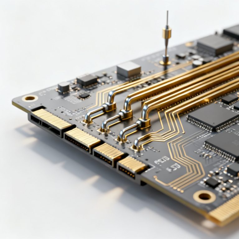
Capturing an eye diagram PCB using an oscilloscope is the definitive method for validating signal integrity in high-speed digital designs. This step-by-step guide covers essential equipment, precise triggering techniques, and advanced analysis to help you measure and troubleshoot your high-speed PCB prototypes effectively.
In the world of high-speed digital design, signal integrity (SI) is paramount. As data rates climb into the gigabit-per-second range, traditional time-domain measurements like rise time and jitter become insufficient to fully characterize a signal’s health. The eye diagram—a synchronized overlay of multiple bit periods—provides a holistic, visual representation of signal quality, revealing issues like jitter, noise, crosstalk, and intersymbol interference (ISI).
For engineers designing or testing high-speed printed circuit boards (PCBs)—especially those featuring High Speed interfaces like HDMI, USB 3.0, PCIe, or DDR memory—capturing an accurate eye diagram is a critical validation step. This comprehensive guide will walk you through the entire process, from equipment setup to advanced analysis, ensuring you can confidently assess your PCB’s signal integrity.
Essential Equipment and Pre-Measurement Setup for Eye Diagram PCB Capture
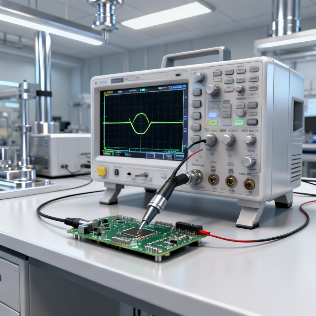
Before connecting probes, ensure you have the right tools. The quality of your eye diagram PCB capture directly depends on the capabilities of your oscilloscope and probes.
Choosing the Right Oscilloscope for Eye Diagram PCB Testing
The oscilloscope’s bandwidth must be at least 3 to 5 times the fundamental clock frequency of the signal. For a 10 Gbps signal, a 33 GHz to 50 GHz oscilloscope is recommended. For lower-speed signals (e.g., 100 MHz clock), a 500 MHz to 1 GHz scope may suffice, but for high-speed serial data, a real-time oscilloscope with a high sample rate (e.g., 40 GS/s or higher) is essential. A minimum sample rate of 2.5 times the signal’s maximum frequency is required to capture enough points per bit for accurate eye reconstruction. For precise jitter and noise analysis, aim for 4x or more. Deep memory (e.g., 100 Mpts or more) allows you to capture long bit sequences, which is critical for analyzing low-frequency jitter and pattern-dependent effects. For most high-speed PCB testing, a real-time digital storage oscilloscope (DSO) is preferred over a sampling oscilloscope. Real-time scopes can capture single-shot events and provide a complete waveform, while sampling scopes require a repetitive trigger and are better for very high-frequency signals (e.g., 40 Gbps+).
Probe Selection and Connection for Accurate Eye Diagrams
Active differential probes are mandatory for high-speed differential signals (e.g., LVDS, USB, HDMI). They provide high bandwidth, low loading, and common-mode rejection. Choose probes with bandwidth matching or exceeding your oscilloscope’s bandwidth. For single-ended signals (e.g., clock lines, single-ended DDR), use a high-impedance active probe. Avoid passive 10x probes for signals above 100 MHz due to their high input capacitance (10-15 pF) which distorts the signal. The probe’s input capacitance (typically 0.3 pF to 1 pF for active probes) must be minimized to avoid corrupting the signal. Always use a probe tip adapter or solder-in probe for the most accurate connection. Avoid long ground leads (the “ground clip”) as they create inductance and ringing. Connect the probe as close to the receiver (RX) pins as possible. The eye diagram measured at the transmitter (TX) may look perfect, but the signal degrades along the PCB trace. Measuring at the RX gives you the true signal that the IC sees.
Oscilloscope Calibration and De-embedding for Eye Diagram PCB Measurement
Perform a probe deskew (also called probe calibration) to match the time delay between two differential probe tips. This is critical for differential signals; a 1 ps skew can reduce the eye opening significantly at 10 Gbps. If you are measuring through a long cable or a test fixture, use the oscilloscope’s de-embedding feature (e.g., S-parameter de-embedding) to remove the effects of the fixture. This provides a true picture of the signal at the PCB trace.
Step-by-Step Procedure to Capture the Eye Diagram PCB
Now, let’s capture the eye diagram PCB. We’ll assume you have a real-time oscilloscope with an active differential probe connected to your High Speed PCB’s differential pair.
Step 1: Configure the Oscilloscope for Eye Diagram PCB Capture
Set the vertical scale so the signal occupies about 70-80% of the screen vertically. For a differential signal, set the vertical scale to about 100-200 mV/div (depending on signal amplitude). Set the time base to show 2 to 3 complete bit periods horizontally. For a 1 Gbps signal (1 ns bit period), set the time base to 500 ps/div or 1 ns/div. This ensures you see the full eye opening. Select the differential channel (e.g., Ch1 – Ch2) or the single-ended channel. Ensure the probe attenuation factor is correctly set in the oscilloscope.
Step 2: Enable the Eye Diagram Mode on Your Oscilloscope
Most modern oscilloscopes have a dedicated Eye Diagram or Serial Data analysis mode. For Keysight (Agilent) Scopes, press the “Analysis” button, then select “Eye/Mask Test” or “Serial Data Analysis.” Choose “Eye Diagram.” For Tektronix Scopes, press the “Analyze” button, then select “Eye Diagram” or “Serial Data Analysis.” You may need to select “Eye Mask” or “Eye Pattern.” For LeCroy Scopes, press the “Analysis” button, then select “Eye Diagram” under the “Serial Data” or “Jitter” menu. If your scope lacks a dedicated eye mode, you can manually create an eye diagram using the Persistence mode. Set persistence to “Infinite” and trigger on the clock. The signal will overlay over time. However, this method lacks advanced analysis tools.
Step 3: Set the Trigger—Crucial for Eye Diagram PCB Accuracy
The trigger is the most critical and often misunderstood part of capturing an eye diagram PCB. For clocked signals, if you have a separate clock signal (e.g., a clock line in DDR), trigger on the clock’s rising edge. Use a clock recovery algorithm if possible. A simple edge trigger on the clock will work, but it may not be stable for high-speed data. For embedded clock signals (e.g., PCIe, USB 3.0, SATA), you must use Clock Recovery. The oscilloscope’s firmware will extract the clock from the data stream using a Phase-Locked Loop (PLL). Set the PLL bandwidth to the standard-specific value (e.g., 10 MHz to 20 MHz for PCIe Gen3). A lower bandwidth (e.g., 1 MHz) will track low-frequency jitter; a higher bandwidth (e.g., 100 MHz) will track high-frequency jitter. For general analysis, start with the standard’s recommended bandwidth. Enter the nominal data rate (e.g., 5 Gbps for USB 3.0). The oscilloscope uses this to determine the bit period (UI). For advanced pattern-dependent analysis (e.g., analyzing ISI), you can trigger on a specific bit pattern (e.g., PRBS7, PRBS15, or a custom pattern). Most scopes allow you to set a “Trigger on Pattern” or “Pattern Lock” mode. This is useful for debugging problems like “long run of zeros” causing baseline wander.
Step 4: Adjust the Eye Diagram Parameters
Once the eye diagram is displayed, fine-tune the settings. Set the number of bit periods to display; usually, 2 to 3 UIs are sufficient. More UIs (e.g., 10) can show pattern-dependent jitter but may make the eye look crowded. Set persistence to Infinite or Long to accumulate many bit transitions. This reveals the “fuzzy” areas showing jitter and noise. For a clean eye, use “Variable Persistence” (e.g., 1 second) to see the average. If you have a compliance mask (e.g., USB 3.0, HDMI 2.0), load it into the scope. The scope will automatically flag any violations (hits inside the mask). This is essential for pass/fail testing.
Step 5: Capture and Analyze the Eye Diagram PCB
Press “Run/Stop” and let the oscilloscope run for a few seconds to accumulate enough data. Then press “Stop” to freeze the eye diagram. Use the horizontal and vertical controls to zoom into the eye opening. Look for Eye Height (the vertical opening, voltage margin), Eye Width (the horizontal opening, time margin), Eye Amplitude (the peak-to-peak voltage of the eye), and Rise Time and Fall Time (measured from the eye’s transition edges, 10%-90%).
Advanced Analysis and Troubleshooting for Eye Diagram PCB
A simple eye diagram can tell you if the signal is “good” or “bad.” Advanced analysis tells you why.
Jitter Decomposition for Eye Diagram PCB Debugging
Jitter is the deviation of the signal’s edges from their ideal timing positions. It is the primary killer of high-speed signals. Use the oscilloscope’s Jitter Analysis software to break jitter into components. Random Jitter (Rj) is caused by thermal noise, shot noise, and other random processes; it is unbounded and follows a Gaussian distribution. Deterministic Jitter (Dj) is caused by specific, repeatable sources. Data-Dependent Jitter (DDJ), also called Intersymbol Interference (ISI), is caused by the bandwidth limitations of the channel (PCB traces, vias, connectors). Long runs of identical bits cause the signal to not reach full voltage, leading to edge timing shifts. Periodic Jitter (Pj) is caused by periodic noise sources like power supply ripple, crosstalk from a nearby clock, or switching regulators. Duty Cycle Distortion (DCD) is caused by a mismatch in the rising and falling edge speeds or a threshold offset in the receiver; the eye will appear asymmetric. Total Jitter (Tj) is usually reported at a specific Bit Error Rate (BER), e.g., Tj @ BER = 1e-12. This is the jitter that the receiver must tolerate. To decompose, use the oscilloscope’s “Jitter Decomposition” or “Jitter Spectrum” function. The spectrum plot shows you the frequency of the periodic jitter, allowing you to identify the source (e.g., a 100 MHz switching regulator).
Noise Analysis in Eye Diagram PCB Measurements
Noise affects the vertical eye opening. Use the oscilloscope’s Noise Analysis to separate noise into Vertical Noise (the amplitude fluctuations at the center of the eye), Horizontal Noise (the timing fluctuations, jitter), and Crosstalk (look at the eye diagram with the aggressor signal active; if the eye closure changes, crosstalk is present).
Using Eye Masks for Compliance Testing of Eye Diagram PCB
For standards like PCIe, USB, HDMI, and Ethernet, the eye mask defines a forbidden region. If any part of the eye diagram enters this region, the design fails. Load the mask in the oscilloscope by selecting “Mask Test” and loading the standard’s mask file (e.g., “USB_3.2_Gen1.mask”). Set the mask tolerance to a margin (e.g., 10% or 20%) to ensure you have design headroom. Run the test; the scope will count the number of hits inside the mask. A passing result is zero hits. If you get hits, use the Mask Violation Histogram to see where the hits occur. For example, hits near the center indicate noise; hits on the edges indicate jitter.
Common Pitfalls and How to Fix Them in Eye Diagram PCB Testing
| Problem | Eye Diagram Appearance | Likely Cause | Solution |
|---|---|---|---|
| Eye Closure (Small Opening) | Narrow vertical and horizontal opening | Excessive jitter, noise, or ISI | Check PCB trace impedance, reduce trace length, add termination, improve power supply filtering |
| Double Eye (Two overlapping eyes) | Two distinct eye openings, one smaller | Duty Cycle Distortion (DCD) | Check for unequal rise/fall times, adjust driver pre-emphasis, verify receiver threshold |
| Fuzzy/Noisy Eye | Thick, blurry traces on the eye edges | Random jitter or high-frequency noise | Improve power supply decoupling, use lower-noise LDOs, add ferrite beads |
| Eye Crossing | The eye does not close completely at the crossing point | Overshoot or ringing due to impedance mismatch | Add series termination (e.g., 33-50 ohm resistor) near the driver, improve PCB stackup |
| Baseline Wander | The eye’s top and bottom levels drift over time | AC coupling or long runs of identical bits | Use DC coupling with proper termination, or adjust the driver’s equalization (e.g., pre-emphasis) |
| Clock Recovery Failure | No eye diagram appears, or the eye is unstable | Incorrect data rate, PLL bandwidth, or signal-to-noise ratio | Double-check the data rate, reduce PLL bandwidth, ensure the signal amplitude is above the scope’s trigger threshold |
Best Practices for High-Speed PCB Design and Eye Diagram Testing
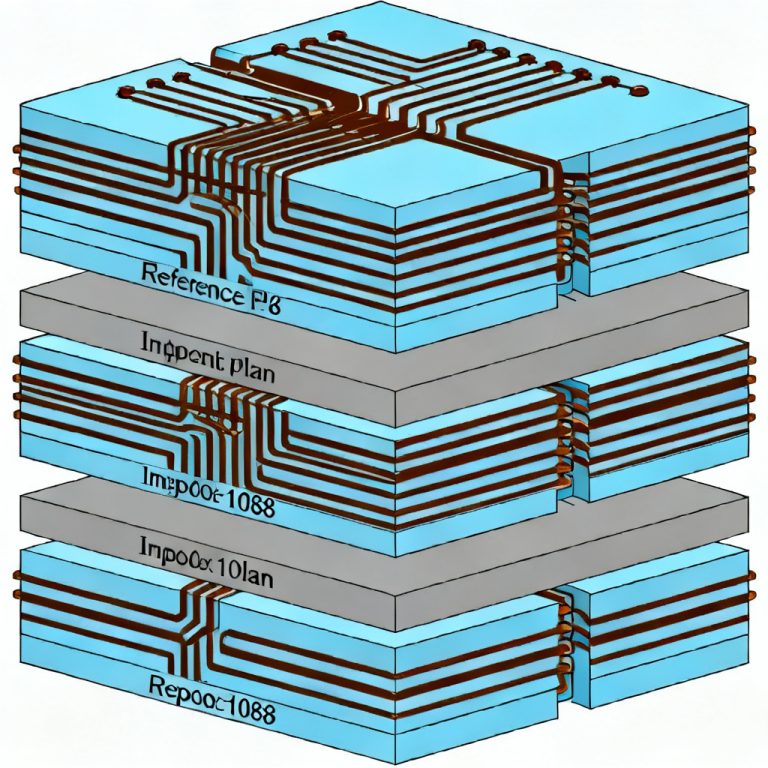
To ensure your eye diagram passes compliance and your design is robust, follow these best practices. Include test points (e.g., small pads or via-in-pad) near the receiver pins. Use SMA connectors or high-speed header for differential pairs if you plan to use external cables. Ensure your PCB traces have a characteristic impedance of 50 ohms (single-ended) or 100 ohms (differential) with a tolerance of +/- 10%. Use a Time Domain Reflectometer (TDR) to verify impedance. Avoid long stubs on high-speed traces. Use back-drilling to remove unused via stubs. A clean power supply is essential. Use multiple decoupling capacitors (e.g., 100 nF, 1 uF, 10 uF) near each IC. Measure the power supply noise at the IC’s pins; it should be less than 1% of the supply voltage. Use SI simulation tools (e.g., ADS, HyperLynx, CST) to predict the eye diagram before building the PCB. This saves time and cost. Test the eye diagram at the worst-case operating conditions (e.g., minimum supply voltage, maximum temperature). The eye will close under stress.
Understanding Key Terminology for Eye Diagram PCB Analysis
To deepen your expertise in eye diagram PCB measurement, it is essential to understand the following industry terms. Signal Integrity (SI) refers to the quality of an electrical signal as it travels through a PCB trace. Intersymbol Interference (ISI) is a form of signal distortion where one symbol interferes with subsequent symbols, often due to channel bandwidth limitations. Jitter is the timing deviation of signal edges from their ideal positions, which can be decomposed into random and deterministic components. Clock Recovery is the process of extracting a timing reference from a data stream, critical for embedded clock signals like PCIe and USB. Eye Mask is a predefined region on an eye diagram that must remain free of signal traces for compliance with industry standards. De-embedding is a technique used to mathematically remove the effects of test fixtures or cables from measurement results. Probe Deskew is the calibration process that aligns the time delays between two differential probe tips. Bit Error Rate (BER) is the number of bit errors divided by the total number of transferred bits, often used to quantify the reliability of a high-speed link.
Why Choose Our High-Speed PCB Services for Eye Diagram Compliance
Our high-speed PCB manufacturing and design services are optimized for superior signal integrity, ensuring your eye diagram measurements consistently pass compliance standards. Unlike generic PCB fabricators, we specialize in controlled impedance, advanced stackup design, and rigorous testing to minimize jitter, crosstalk, and ISI. Our engineering team provides free design reviews to help you achieve the cleanest eye diagram possible, from prototype to production. We offer 50 ohm and 100 ohm impedance control with tight tolerances, back-drilling for via stubs, and high-frequency material selection to support data rates up to 112G. By partnering with us, you gain a dedicated partner committed to your high-speed PCB success.
Frequently Asked Questions About Eye Diagram PCB Capture
What is an eye diagram in PCB testing?
An eye diagram in PCB testing is a synchronized overlay of multiple bit periods of a digital signal, captured using an oscilloscope. It provides a visual representation of signal quality, revealing issues like jitter, noise, and intersymbol interference (ISI) in high-speed PCB designs.
How do I capture an eye diagram PCB using an oscilloscope?
To capture an eye diagram PCB, connect a high-bandwidth oscilloscope and active probe to the receiver pins of your PCB. Enable the eye diagram mode, set up clock recovery for embedded signals, adjust the time base to show 2-3 bit periods, and run the acquisition. Analyze the eye height, width, and jitter to assess signal integrity.
What equipment is needed for eye diagram PCB measurement?
For eye diagram PCB measurement, you need a real-time oscilloscope with bandwidth at least 3-5 times the signal’s clock frequency, active differential probes, and a probe tip adapter for accurate connection. Optional tools include a TDR for impedance verification and simulation software for pre-layout analysis.
Why is clock recovery important for eye diagram PCB capture?
Clock recovery is crucial for eye diagram PCB capture because many high-speed interfaces like PCIe and USB 3.0 embed the clock within the data stream. Without proper clock recovery using a PLL, the oscilloscope cannot synchronize the bit periods, resulting in an unstable or unusable eye diagram.
How can I improve the eye diagram of my high-speed PCB?
To improve the eye diagram of your high-speed PCB, ensure controlled impedance (50 ohm or 100 ohm), minimize trace stubs with back-drilling, use proper termination, and optimize power supply decoupling. Simulate the design before fabrication and test at worst-case conditions to ensure robust signal integrity.