Mastering Time Interval Error analysis for jitter in high speed PCB is essential for signal integrity engineers targeting reliable multi-gigabit data transmission. This guide consolidates expert methodologies to help you quantify, decompose, and mitigate timing deviations effectively.
What is Time Interval Error and Why It Matters for Jitter in High Speed PCB
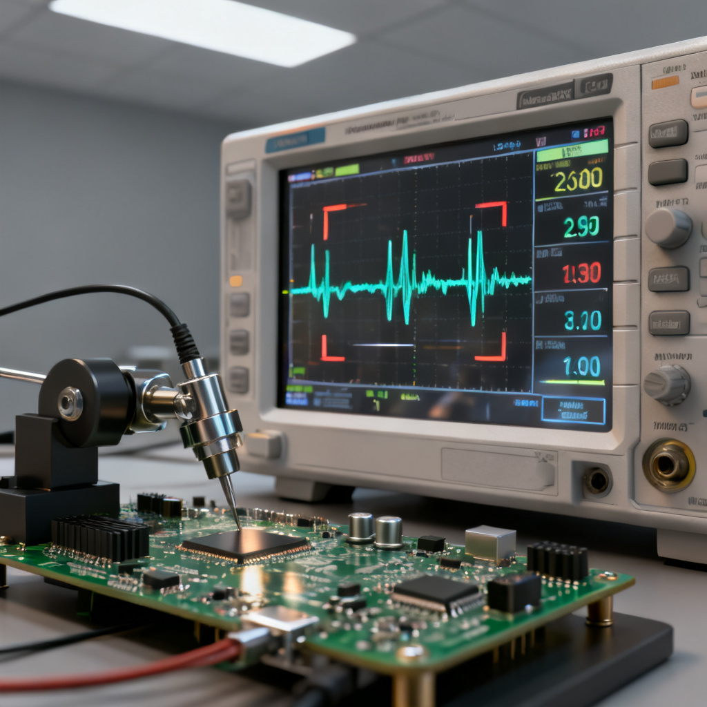
Time Interval Error (TIE) is the measurement of the difference between the actual timing of a signal edge and its ideal expected position. This fundamental building block of jitter in high speed PCB design captures cumulative timing deviations over time, unlike period jitter or cycle-to-cycle jitter. TIE analysis provides the raw data from which all jitter metrics are derived:
- Total Jitter (TJ): The peak-to-peak value of the TIE histogram.
- Deterministic Jitter (DJ): The bounded predictable component caused by crosstalk, SSN, and ISI.
- Random Jitter (RJ): The unbounded Gaussian component attributed to thermal and flicker noise.
- Phase Noise: The frequency-domain equivalent of TIE, revealing specific noise sources from PLLs or voltage regulators.
TIE is the only metric that allows separation of jitter into its constituent parts, making it indispensable for root cause analysis in high speed PCB troubleshooting.
Direct Link Between TIE and Jitter Types
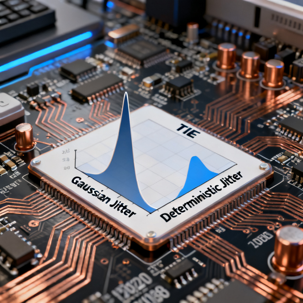
Understanding the relationship between TIE and various jitter types is critical for high speed PCB design. The TIE histogram’s shape directly indicates the dominant jitter mechanism: a Gaussian distribution suggests random jitter, while bi-modal or multi-peak distributions indicate deterministic jitter from specific sources like power supply noise or impedance mismatches.
How to Measure TIE: Methodology and Best Practices
Accurate TIE measurement requires proper equipment and rigorous methodology. The following steps ensure reliable jitter characterization for high speed PCB validation.
Essential Equipment for TIE Measurement
| Equipment | Role in TIE Analysis for Jitter in High Speed PCB | Key Specification |
|---|---|---|
| Real-Time Oscilloscope (DSO) | Captures continuous waveform for TIE extraction | Memory depth for long captures |
| Time Interval Analyzer (TIA) | High-precision timing measurements | Measurement speed and resolution |
| BERT | System-level jitter tolerance testing | Data rate and pattern generation |
Step-by-Step Measurement Process
- Connect and Configure: Probe the test point with appropriate vertical scale (100-200 mV/div).
- Set the Reference Clock: Use clock recovery for data signals; configure PLL per standard (e.g., PCIe Gen 4, USB 3.2).
- Acquire Data: Capture at least 1 million UI for statistically valid RJ measurement.
- Perform TIE Extraction: Use oscilloscope jitter analysis software to compare crossing points to ideal positions.
- Generate Jitter Histogram: The histogram of all TIE values forms the basis for decomposition.
Best Practices for Accurate Measurement
- Probe Loading: Use low-capacitance active probes (≤0.3 pF) to minimize circuit impact.
- Grounding: Use short, low-inductance ground leads to avoid noise pickup.
- Averaging: Do not use waveform averaging; it removes random jitter.
- Statistical Significance: Capture millions of edges for reliable TJ extrapolation.
Decomposing Jitter from TIE Data: The Expert Approach
Once raw TIE data is obtained, decomposition into root causes is the next critical step for high speed PCB optimization.
The TIE Trend Plot as Diagnostic Tool
The TIE trend plot (TIE vs. time) reveals jitter characteristics:
- Flat, Noisy Line: Indicates primarily Random Jitter (RJ) from thermal noise.
- Sinusoidal Pattern: Indicates Periodic Jitter (PJ); frequency identifies source (e.g., 1.5 MHz from switching power supply).
- Patterned/Data-Dependent Pattern: Indicates Data-Dependent Jitter (DDJ) from Inter-Symbol Interference (ISI).
- Step Change or Drift: Indicates Duty Cycle Distortion (DCD) or wander from temperature changes.
Dual-Dirac Model for RJ and DJ Extraction
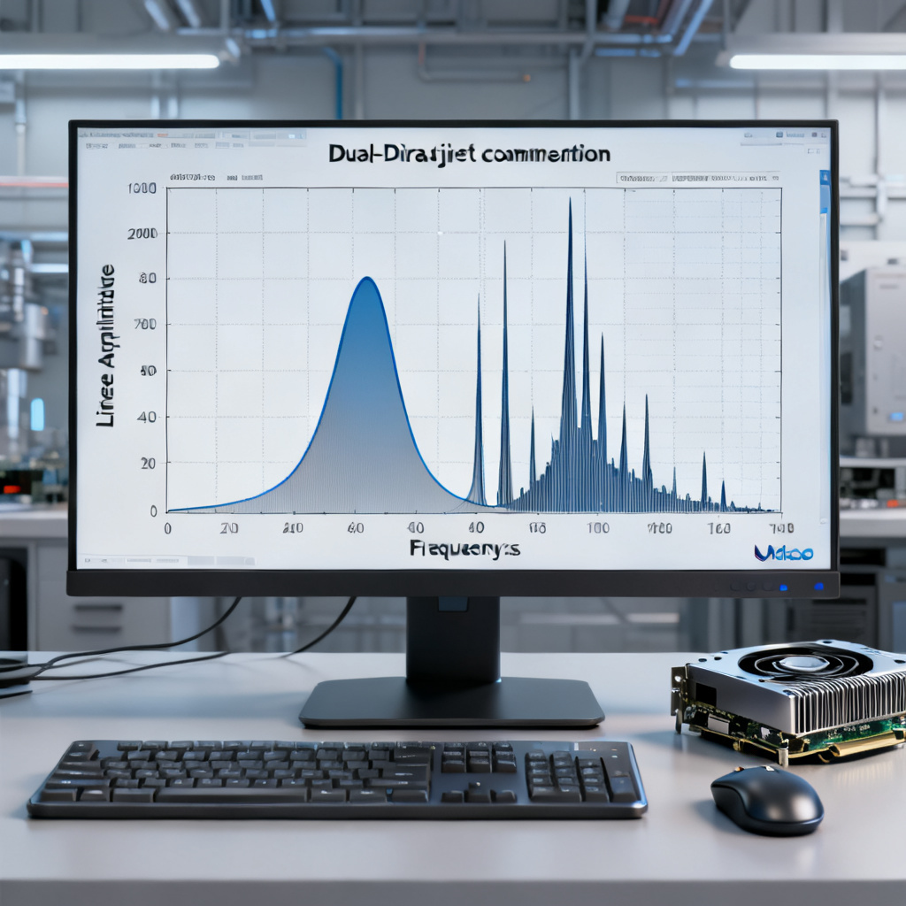
The Dual-Dirac model fits Gaussian curves to the tails of the TIE histogram. The distance between the means of two Gaussians is Deterministic Jitter (DJ); their standard deviation is Random Jitter (RJ RMS). Total Jitter (TJ) is calculated as: TJ = DJ + 2 × n × RJ(RMS), where n is the crest factor for target BER (e.g., 14.069 for BER 10⁻¹²).
Advanced Decomposition Techniques
- BERT Scan: Creates bathtub curves showing eye opening at target BER; slope reveals RJ/DJ ratio.
- Jitter Spectrum (Phase Noise Plot): Converts TIE data to frequency domain, revealing spurs at specific frequencies (e.g., 100 MHz from system clock, 1.5 MHz from buck converter).
Practical Application: Debugging Jitter in Your High Speed PCB
Apply TIE analysis systematically to resolve common high speed PCB jitter issues.
Isolating Periodic Jitter from Power Supply Noise
Problem: High BER on 10 Gbps serial link. TIE Analysis: Clear 1.5 MHz sinusoidal pattern in trend plot. Root Cause: Switching power supply noise coupling into PLL. Action: Add decoupling capacitors near power supply and sensitive PLL; use ferrite bead; re-route power trace away from data lanes.
Diagnosing ISI from Channel Loss
Problem: Closed eye diagram for long bit runs. TIE Analysis: Data-dependent pattern with bathtub-shaped histogram. Root Cause: Inter-Symbol Interference (ISI) from high insertion loss and reflections. Action: Reduce trace length; ensure impedance matching (50Ω or 100Ω differential); use pre-emphasis/de-emphasis driver; add CTLE or DFE equalization.
Identifying Duty Cycle Distortion
Problem: Asymmetrical eye diagram with crossing point not at 50% amplitude. TIE Analysis: Two distinct histogram peaks with small bounded jitter; pattern repeating every two bits. Root Cause: Duty Cycle Distortion (DCD) from driver rise/fall time mismatch or receiver threshold offset. Action: Check driver transistor sizing; verify receiver threshold; use differential signaling (LVDS, CML) for inherent DCD immunity.
Best Practices for Minimizing Jitter in Your PCB Design
Preventative design practices significantly reduce jitter in high speed PCB implementations.
- Power Integrity: Use low-impedance PDN with multiple decoupling capacitors; keep power and ground planes close.
- Controlled Impedance Routing: Route high-speed traces as transmission lines with controlled impedance; avoid 90-degree corners.
- Minimize Crosstalk: Keep high-speed traces away from noisy signals; use guard traces and ground vias; maintain 3W rule spacing.
- Differential Signaling: Use differential pairs (LVDS, CML, PCIe) for common-mode noise rejection.
- Proper Termination: Terminate all high-speed traces at receiver to prevent reflections.
- Low-Jitter Components: Select oscillators, PLLs, and clock buffers with <1 ps RMS jitter; use dedicated clean power supply for clocking.
Comparison: TIE Analysis vs. Alternative Jitter Measurement Methods
| Method | Advantages for Jitter in High Speed PCB | Limitations |
|---|---|---|
| TIE Analysis | Provides cumulative timing deviation; enables RJ/DJ decomposition; identifies root causes | Requires long capture memory; complex setup for clock recovery |
| Period Jitter | Simple to measure; good for clock jitter | Does not capture cumulative effects; misses low-frequency jitter |
| Cycle-to-Cycle Jitter | Useful for PLL characterization | Not suitable for data-dependent jitter analysis |
| BERT Scan | Direct BER measurement; system-level validation | Does not provide root cause information |
At [Your Company Name], we specialize in high speed PCB design and fabrication with advanced TIE analysis capabilities. Our engineering team ensures your boards meet stringent signal integrity requirements for data rates up to 112 Gbps PAM-4.
FAQ: Time Interval Error Analysis for Jitter in High Speed PCB
What is the difference between TIE and period jitter in high speed PCB design?
TIE measures cumulative timing deviation from ideal over time, while period jitter measures variation in one clock period. TIE is essential for analyzing long-term jitter effects like wander and phase noise in high speed PCB systems.
How many UI are needed for accurate TIE analysis in high speed PCB?
At least 1 million UI (Unit Intervals) are recommended for statistically valid random jitter measurement. For example, at 10 Gbps, this requires a 100-microsecond capture record.
Can TIE analysis identify crosstalk-induced jitter in high speed PCB?
Yes. TIE analysis can reveal periodic jitter patterns in the trend plot, and the jitter spectrum (phase noise plot) will show spurs at the crosstalk aggressor frequency, enabling precise identification of crosstalk sources.
What equipment is best for TIE measurement in high speed PCB?
A real-time oscilloscope with deep memory depth is most common and versatile. For production testing, a Time Interval Analyzer (TIA) offers faster measurement speeds. BERTs are used for system-level validation.
How does TIE analysis help reduce jitter in high speed PCB manufacturing?
By decomposing jitter into RJ, DJ, PJ, ISI, and DCD components, TIE analysis pinpoints root causes such as power supply noise, impedance mismatches, or crosstalk. This enables targeted design improvements during PCB fabrication.