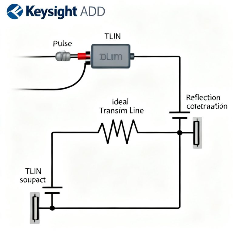
In high-speed digital systems, the clock distribution network is the heartbeat of the entire design. Understanding jitter transfer and generation in high speed PCB clock distribution networks is critical for reliable multi-gigabit performance. This pillar page provides a deep, technical dive into jitter mechanisms, measurement techniques, and practical design strategies.
Understanding Jitter Fundamentals in High Speed PCB Clock Distribution Networks
Jitter is the short-term, non-cumulative variation of a digital signal’s significant instants from their ideal positions in time. In high speed PCB clock distribution networks, jitter manifests in two primary forms: Jitter Transfer (JTRAN) and Jitter Generation.
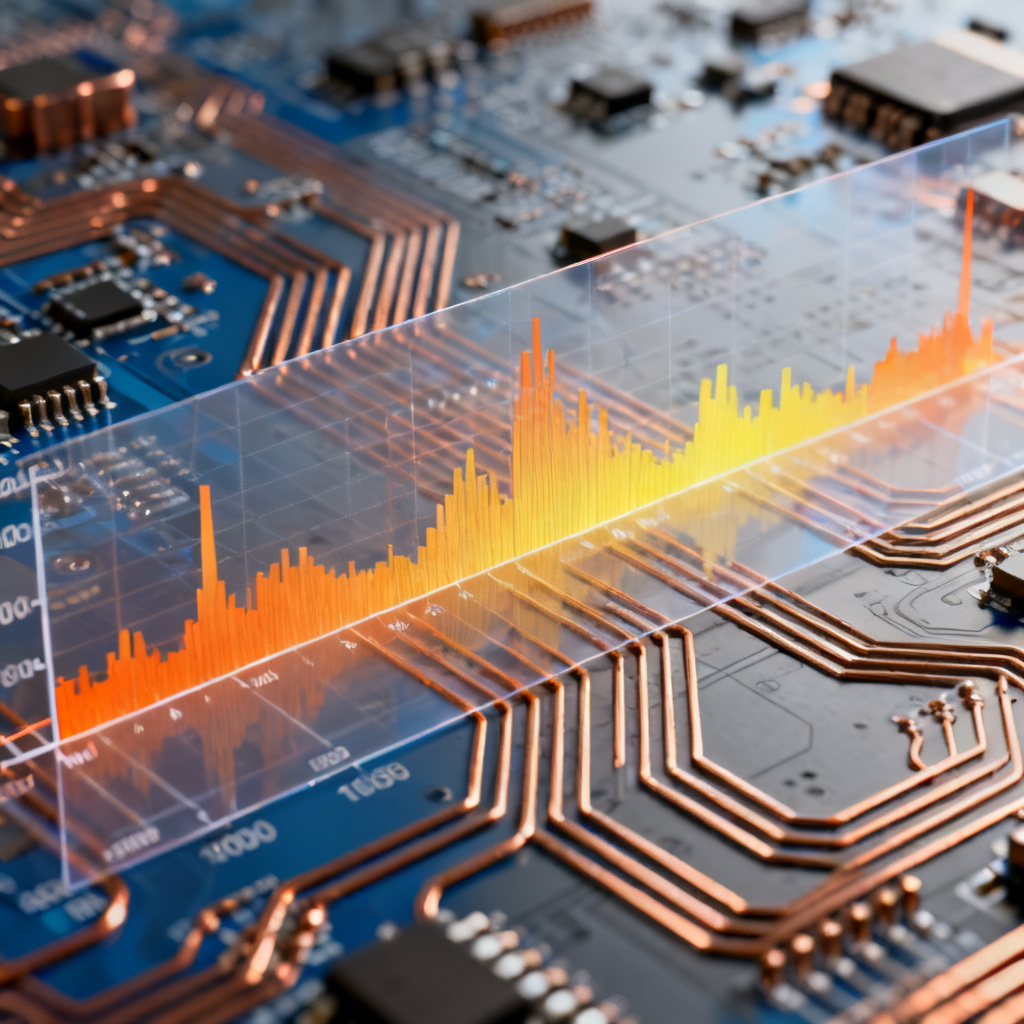
Key Jitter Types in High-Speed Networks
- Random Jitter (RJ): Gaussian in nature, unbounded, caused by thermal and shot noise.
- Deterministic Jitter (DJ): Bounded and predictable, including Periodic Jitter (PJ), Data-Dependent Jitter (DDJ), and Duty Cycle Distortion (DCD).
Jitter transfer describes how input jitter propagates through PLLs and buffers. Jitter generation refers to intrinsic jitter produced by components even with a clean input.
Jitter Transfer Mechanisms in High Speed PCB Clock Distribution Networks
Jitter transfer is a critical specification for PLLs and clock buffers. A PLL acts as a low-pass filter for input jitter, with bandwidth and peaking characteristics that directly affect jitter transfer in high speed PCB clock distribution networks.
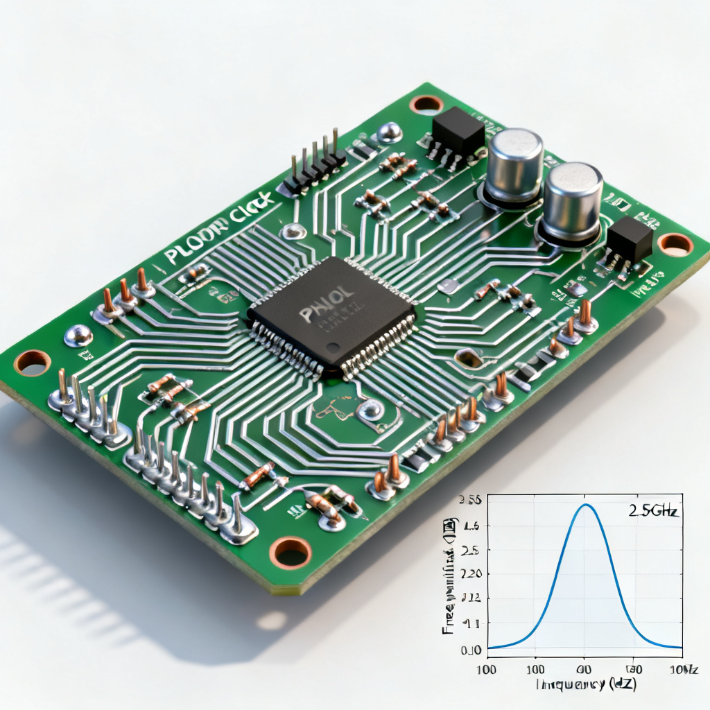
PLL Jitter Transfer Characteristics
- Low-Frequency Jitter: Below PLL bandwidth, jitter transfers 1:1.
- High-Frequency Jitter: Above bandwidth, the loop filter attenuates jitter.
- Jitter Peaking: Near the natural frequency, amplification can occur.
Buffer-Induced Jitter Transfer
Clock buffers transfer jitter based on Power Supply Rejection Ratio (PSRR) and crosstalk susceptibility. Poor PSRR allows power supply noise to modulate buffer delay.
Channel-Induced Jitter Transfer
PCB traces act as transmission lines. Skin effect, dielectric loss, and impedance discontinuities create ISI and deterministic jitter.
Root Causes of Jitter Generation in High Speed PCB Designs
Jitter generation originates from active components and passive interconnect. Key sources include:
Intrinsic Jitter from Oscillators and PLLs
- Crystal Oscillators: Phase noise translates to random jitter.
- PLL Phase Noise: VCO susceptibility to power supply noise.
Power Supply Induced Jitter (PSIJ)
Noise on power rails modulates CMOS gate delay. A buffer with 1 ps/mV sensitivity generates 10 ps of jitter from 10 mV of ripple.
Substrate and Ground Bounce
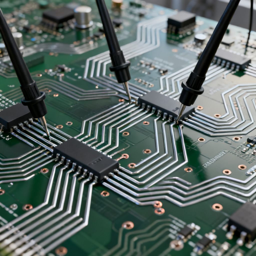
Digital switching noise couples into analog clock circuitry. Simultaneous Switching Outputs (SSO) cause ground reference shifts.
Thermal and Flicker Noise
Thermal noise contributes to random jitter. Flicker noise dominates at low frequencies, contributing to long-term wander.
Practical Design Strategies to Minimize Jitter Transfer and Generation
Engineers must address both transfer and generation mechanisms simultaneously for optimal jitter transfer and generation in high speed PCB clock distribution networks.
Component Selection and Topology
- Use low-jitter PLLs and buffers with specified RMS jitter values.
- Avoid cascading PLLs; if necessary, use different bandwidths.
- Implement a clean clock tree with a single master oscillator.
Power Supply Integrity (PSI)
- Dedicated low-noise LDOs with high PSRR.
- Proper decoupling with multiple capacitor values.
- Isolated power plane for clock circuits.
PCB Layout and Routing
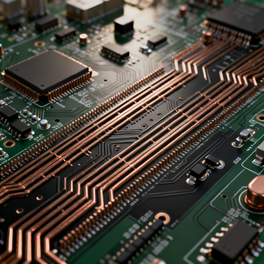
- Controlled impedance traces (50 Ω microstrip or stripline).
- Minimize trace length; use differential signaling for long runs.
- Guard traces, ground planes, and 3W spacing rule.
- Minimize vias; use back-drilling if necessary.
Clock Termination and Signal Integrity
- Proper termination to prevent reflections.
- Use differential signaling (LVDS, CML) above 100 MHz.
- AC-coupling for inter-board connections.
Jitter Measurement and Verification
- Real-time oscilloscope with jitter analysis software.
- Phase noise analyzer for sub-1 ps RMS jitter.
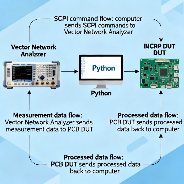
- Jitter transfer function measurement using network analyzer.
Jitter Performance Comparison: Key Parameters
| Parameter | Impact on Jitter Transfer and Generation | Design Target |
|---|---|---|
| PLL Bandwidth | Controls jitter transfer cutoff frequency | 100 kHz – 1 MHz |
| PSRR (1 MHz) | Rejects power supply noise | >60 dB |
| Trace Impedance | Minimizes reflections and ISI | 50 Ω ±10% |
| Buffer Jitter Generation | Intrinsic output jitter | <0.1 ps RMS |
| Differential Pair Skew | Reduces common-mode conversion | <5 ps |
Advanced Considerations: Jitter in High-Speed Serial Links
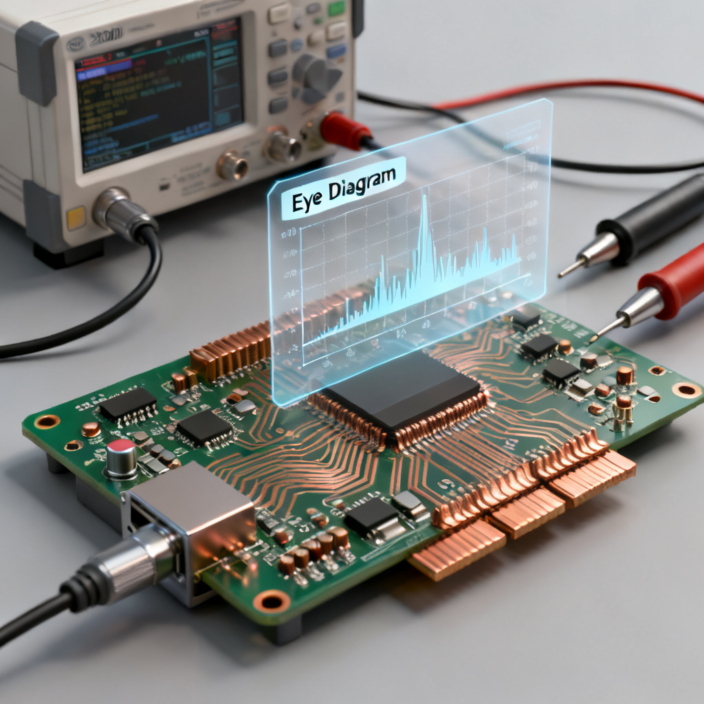
For PCIe, Gigabit Ethernet, and SerDes, jitter is measured as Total Jitter (TJ) at a specific BER. Jitter transfer and generation in high speed PCB clock distribution networks directly affects eye diagram closure and CDR lock.
Key Concepts
- Eye Diagram: Clock jitter closes the eye horizontally.
- Clock Recovery (CDR): Acts as a high-pass filter for jitter.
- Compliance Testing: Standards like PCIe Gen 5 require specific jitter limits.
Glossary of Key Terms
- Jitter Transfer (JTRAN): The ability of a network to pass jitter from input to output.
- Jitter Generation: Intrinsic jitter produced by components.
- PSIJ (Power Supply Induced Jitter): Jitter caused by power rail noise.
- PLL (Phase-Locked Loop): A feedback system that generates a stable clock.
- CDR (Clock and Data Recovery): Circuit that extracts clock from data stream.
Frequently Asked Questions about Jitter Transfer and Generation in High Speed PCB Clock Distribution Networks
What is the difference between jitter transfer and jitter generation?
Jitter transfer describes how input jitter propagates through a network, while jitter generation refers to intrinsic jitter produced by components even with a clean input. Both are critical for jitter transfer and generation in high speed PCB clock distribution networks.
How does power supply noise affect jitter in clock distribution?
Power supply noise modulates gate delays in buffers and PLLs, causing Power Supply Induced Jitter (PSIJ). Using LDOs with high PSRR and proper decoupling minimizes this effect in high speed PCB clock distribution networks.
What is jitter peaking in PLLs?
Jitter peaking is amplification of input jitter near the PLL’s natural frequency. It is critical to control peaking below 0.1 dB in cascaded networks to avoid jitter amplification.
How can I measure jitter in my clock distribution network?
Use a real-time oscilloscope with jitter analysis software for general measurements, or a phase noise analyzer for sub-1 ps RMS jitter. Jitter transfer function can be measured with a network analyzer.
What are the best practices for reducing jitter in PCB layout?
Use controlled impedance traces, minimize trace length, implement guard traces, avoid vias, and use differential signaling. Proper termination and power supply integrity are also essential.
Conclusion
Mastering jitter transfer and generation in high speed PCB clock distribution networks is essential for reliable high-speed system design. By understanding jitter mechanisms, selecting low-jitter components, ensuring robust power integrity, and implementing careful PCB layout, engineers can achieve optimal timing performance. As data rates continue to climb, these principles remain critical for success.
Need a custom high-speed PCB with optimized clock distribution? Our engineering team specializes in low-jitter designs for multi-gigabit applications. Contact us for a free design review or quote.