An Eye Diagram PCB for USB4 compliance is a critical signal integrity test that visually verifies the quality of high-speed differential signals at 10 Gbps (Gen 2) or 20 Gbps (Gen 3) per lane. This pillar content provides a comprehensive guide to specifications, test setup, and PCB design considerations for achieving a compliant eye diagram.
What Is an Eye Diagram in PCB Design for USB4?
An Eye Diagram PCB is a visual representation of a digital signal’s quality over time, created by overlaying multiple bit periods (typically a PRBS pattern) on an oscilloscope. In high-speed PCB design, it reveals critical signal integrity metrics such as jitter, noise, rise/fall times, and voltage levels. For USB4, the eye diagram must meet strict compliance thresholds to ensure reliable data transmission at 10 Gbps (Gen 2) or 20 Gbps (Gen 3) per lane.
The diagram’s “eye” shape—an open area in the center—indicates a clean signal. A closed eye suggests degradation due to issues like impedance mismatches, crosstalk, or excessive jitter. For USB4, the eye must be open at the receiver input, with specific voltage and timing margins defined by the USB4 specification.
Why Eye Diagram Testing Is Critical for USB4 Compliance
USB4 compliance testing is mandatory for certification. The Eye Diagram PCB test verifies that the signal from a USB4 transmitter (e.g., a host or device) meets the electrical specifications at the test point, typically at the connector or after a reference channel. Failure to pass can lead to data errors, re-transmissions, or product rejection.
Key reasons include:
- Signal Integrity Validation: Ensures the PCB trace, vias, and connectors do not distort the signal.
- Jitter Analysis: Measures random and deterministic jitter, which must be below USB4 limits.
- Voltage Margin: Confirms the eye opening meets minimum voltage thresholds (e.g., 100 mV for Gen 3).
- Compliance to USB-IF Standards: Required for products to use the USB4 logo.
For PCB designers, understanding these tests helps optimize stackup, trace routing, and material selection (e.g., low-loss laminates like Megtron 6 or Rogers 4350B) to achieve a clean eye.
USB4 Eye Diagram Specifications: What You Need to Know
The USB4 specification, defined by the USB Implementers Forum (USB-IF), outlines strict Eye Diagram PCB parameters. Below are the critical specs for Gen 2 (10 Gbps) and Gen 3 (20 Gbps) signals.
Eye Opening Voltage and Timing
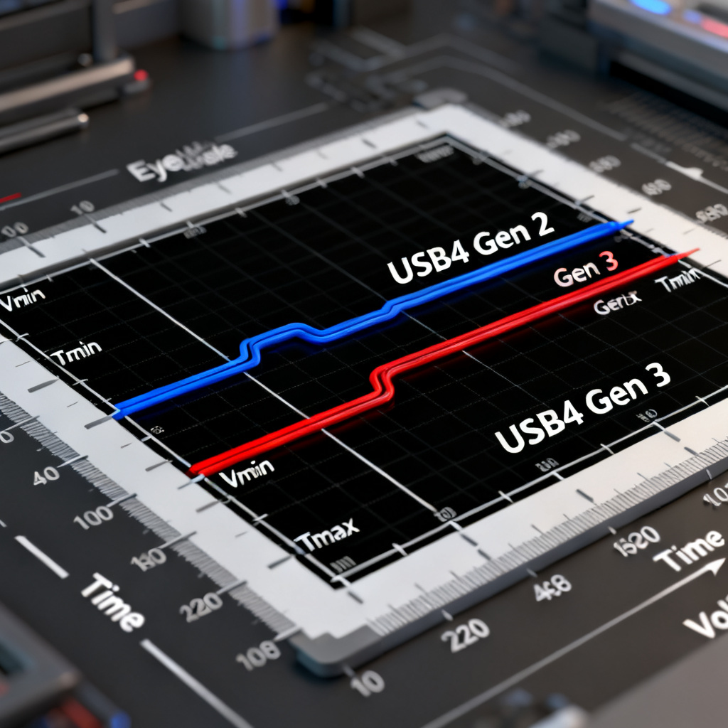
- Gen 2 (10 Gbps): Minimum eye opening at the receiver (after channel loss) is typically 100 mV (differential peak-to-peak) and 0.3 UI (unit interval, where 1 UI = 100 ps). This ensures enough margin for noise.
- Gen 3 (20 Gbps): Minimum eye opening is 100 mV (differential) and 0.2 UI (1 UI = 50 ps). The tighter timing margin reflects higher data rates.
- Test Point: Measured at the connector (TP1 for transmitter) or after a reference channel (TP2 for receiver). The reference channel models PCB trace loss up to 20 dB at Nyquist frequency.
Jitter Limits
Jitter is the deviation from ideal timing. USB4 specifies:
- Total Jitter (TJ): Must be less than 0.3 UI for Gen 2 and 0.2 UI for Gen 3, measured at a bit error rate (BER) of 10^-12.
- Random Jitter (RJ): Typically < 1 ps RMS for Gen 3.
- Deterministic Jitter (DJ): Includes duty cycle distortion (DCD) and data-dependent jitter (DDJ), limited to < 0.15 UI.
Rise/Fall Time
- 20% to 80% rise/fall time: Must be between 15 ps and 30 ps for Gen 3. For Gen 2, the range is 30 ps to 60 ps. Slower edges cause eye closure; faster edges increase EMI.
Differential Voltage Levels
- Peak-to-peak differential voltage (Vdiff): 800 mV to 1.2 V for Gen 2; 400 mV to 600 mV for Gen 3 (reduced swing for lower power).
- Common mode voltage (Vcm): Must be within ±50 mV of 0 V (for AC-coupled links).
Mask Test
The USB4 compliance Eye Diagram PCB uses a mask—a hexagonal or rectangular region in the center of the eye. The signal must not touch the mask boundaries. The mask dimensions are defined in the USB4 spec (e.g., for Gen 3, the mask height is 100 mV, width is 0.2 UI). Any violation fails the test.
| Parameter | Gen 2 (10 Gbps) | Gen 3 (20 Gbps) |
|---|---|---|
| Minimum Eye Opening Voltage | 100 mV | 100 mV |
| Minimum Eye Opening Timing | 0.3 UI | 0.2 UI |
| Total Jitter (TJ) | < 0.3 UI | < 0.2 UI |
| Rise/Fall Time (20%-80%) | 30 ps – 60 ps | 15 ps – 30 ps |
| Differential Voltage (Vdiff) | 800 mV – 1.2 V | 400 mV – 600 mV |
Eye Diagram Test Setup for USB4 Compliance
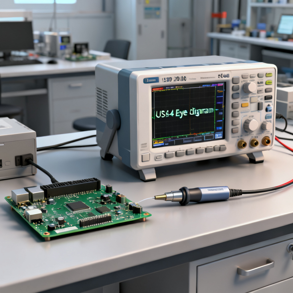
A proper test setup is crucial for accurate Eye Diagram PCB results. Here’s the step-by-step process, based on USB-IF and industry best practices.
Equipment Required
- Real-Time Oscilloscope: Bandwidth of at least 20 GHz (for Gen 3) or 13 GHz (for Gen 2). Use a scope with low noise floor (e.g., Keysight DSAZ204A or Tektronix DPO75902SX).
- Differential Probe: High-impedance, 20+ GHz bandwidth (e.g., Tektronix P7700 or Keysight N2807A). Ensure minimal loading.
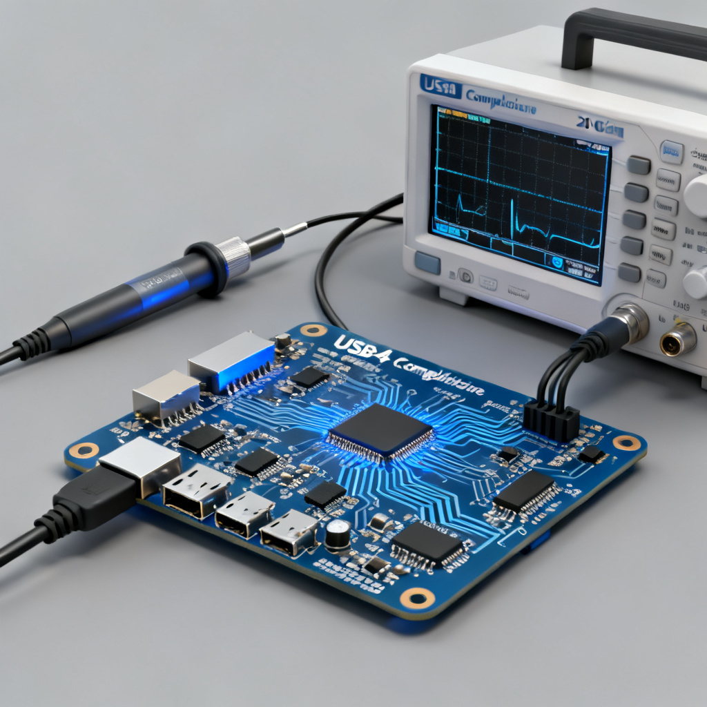
- Test Fixture: A USB4 compliance board (e.g., from Wilder Technologies or USB-IF) that provides SMA or SMPM connectors for probing.
- Signal Generator: For PRBS patterns (e.g., PRBS7 or PRBS31). USB4 uses PRBS9 for jitter testing.
- Software: USB-IF compliance test software (e.g., USB4 Electrical Test Suite from Teledyne LeCroy) or scope-based tools.
Test Setup Steps
- Connect the DUT (Device Under Test): The PCB or cable assembly is connected to the test fixture via the USB4 connector. Ensure the fixture has 50-ohm impedance matching.
- Configure the Signal: The DUT transmits a PRBS9 pattern at the target data rate (10 or 20 Gbps). This pattern mimics real-world data.
- Probe the Signal: Attach the differential probe to the test point (TP1 for transmitter, or after a reference channel for receiver). For PCB testing, probe at the connector pad or a dedicated test via.
- Set Up the Oscilloscope:
- Time base: 50 ps/div for Gen 3, 100 ps/div for Gen 2.
- Vertical scale: 100 mV/div (differential).
- Trigger: On the clock or data pattern (use a clock recovery function if available).
- Acquire the Eye Diagram: Capture at least 1 million UI (for BER 10^-12 confidence). Use persistence mode to overlay waveforms.
- Apply the Mask: Load the USB4 mask (e.g., from USB-IF specification) into the scope software. The mask defines the pass/fail region.
- Measure Jitter and Voltage: Use the scope’s built-in jitter analysis (e.g., TIE (Time Interval Error) and eye measurements). Record TJ, RJ, DJ, and eye height/width.
- Check Compliance: Compare against USB4 limits. If the eye touches the mask, the design fails—requires PCB redesign (e.g., shorter traces, better termination).
Common Test Points in PCB Design
- TP1 (Transmitter): At the output of the USB4 controller IC (after any on-chip termination).
- TP2 (Receiver): At the connector or after a reference channel (simulating PCB loss). For PCB design, test at the via or pad near the connector.
- TP3 (Cable): At the cable’s far end (for cable assemblies).
PCB Design Considerations for a Clean USB4 Eye Diagram
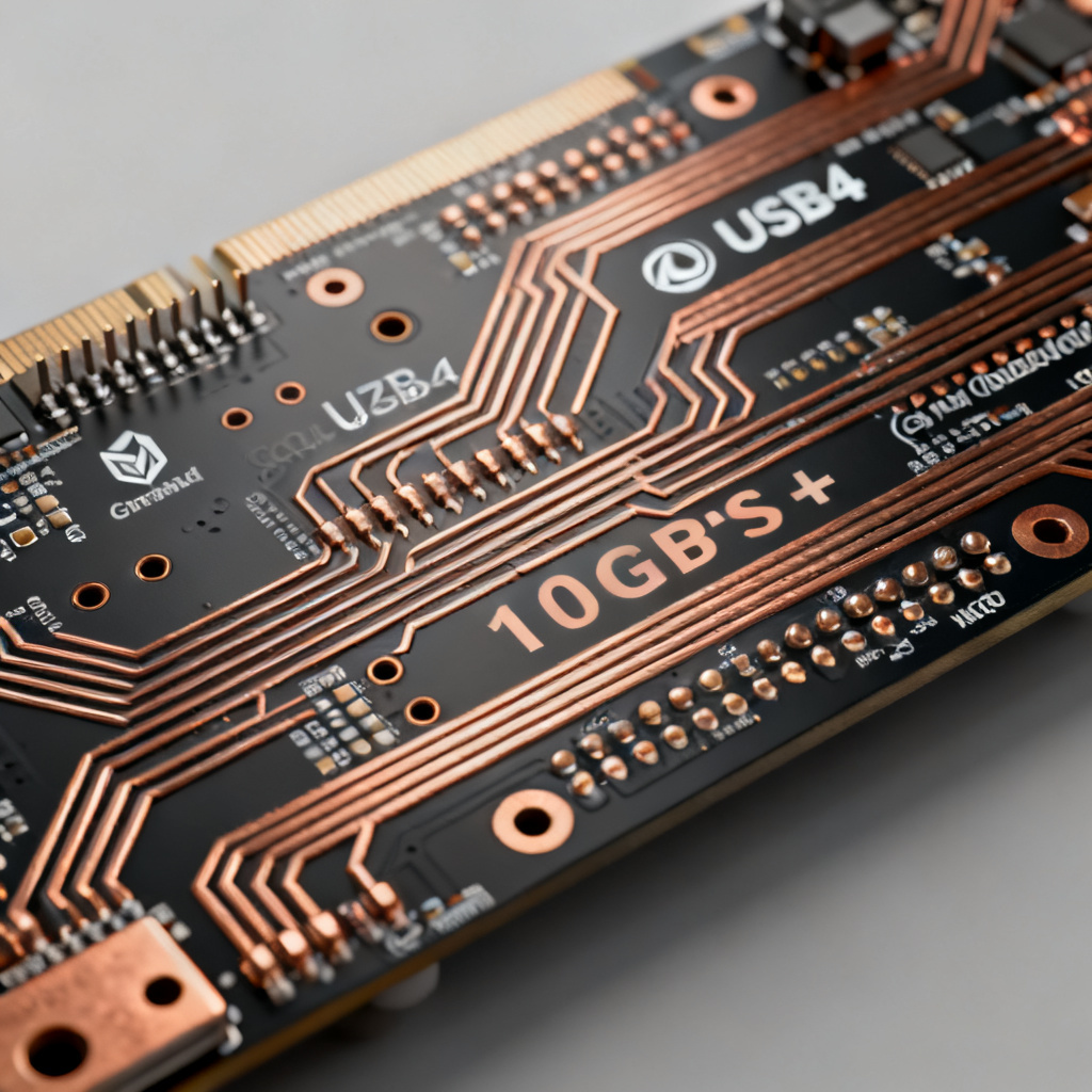
Achieving a compliant Eye Diagram PCB requires careful PCB design. Key factors include:
Impedance Control
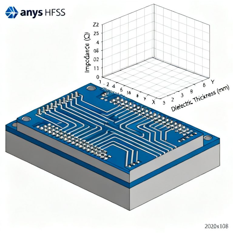
- Target 100 ohms differential impedance ±10% for USB4 traces.
- Use controlled dielectric materials (e.g., FR4 with low Dk tolerance or high-speed laminates). For Gen 3, avoid FR4 due to high loss above 10 GHz.
Trace Routing
- Keep trace lengths as short as possible (< 5 inches for Gen 3).
- Avoid 90-degree bends; use 45-degree or curved routing.
- Maintain symmetric routing for differential pairs (length mismatch < 5 mils).
- Use ground vias near signal vias to reduce inductance.
Via Design
- Use microvias or back-drilled through-holes to minimize stub effects.
- Keep via diameter small (e.g., 8 mils) and pad size consistent.
- Place ground vias within 20 mils of signal vias.
Material Selection
- For Gen 3, use low-loss laminates like Rogers 4350B or Isola I-Speed with Df < 0.005 at 10 GHz.
- For Gen 2, high-quality FR4 (e.g., FR408) may suffice, but verify with simulation.
Termination and AC Coupling
- Use 100 nF AC-coupling capacitors on each lane (near the transmitter or receiver).
- Ensure termination resistors are 50 ohms to ground (for single-ended) or 100 ohms differential.
Power Integrity
- Decouple USB4 power pins with 0.1 µF and 10 µF capacitors.
- Use a solid ground plane beneath high-speed traces.
For comparison, our custom high-speed PCB designs (e.g., High-Speed PCB Design services) use advanced stackup and impedance control to ensure eye diagram compliance, offering faster turnaround and lower cost than generic alternatives.
Interpreting Eye Diagram Results for USB4
After testing, analyze the Eye Diagram PCB for:
- Eye Height: Must be > 100 mV. If low, check for impedance mismatch or excessive PCB loss.
- Eye Width: Must be > 0.2 UI (for Gen 3). If narrow, reduce jitter by improving clock recovery or reducing crosstalk.
- Mask Margin: The distance from the signal to the mask edges. A margin > 10% is ideal.
- Jitter Breakdown: High RJ suggests random noise (e.g., from PLL); high DJ indicates deterministic issues (e.g., reflections, ISI).