Understanding the Eye Diagram PCB for PAM4 signaling is critical for any high-speed PCB designer moving beyond 28 Gbps. This guide explains how PAM4 eye patterns differ from NRZ and what PCB parameters ensure signal integrity.
What Is an Eye Diagram in PCB Testing for PAM4 Signaling?
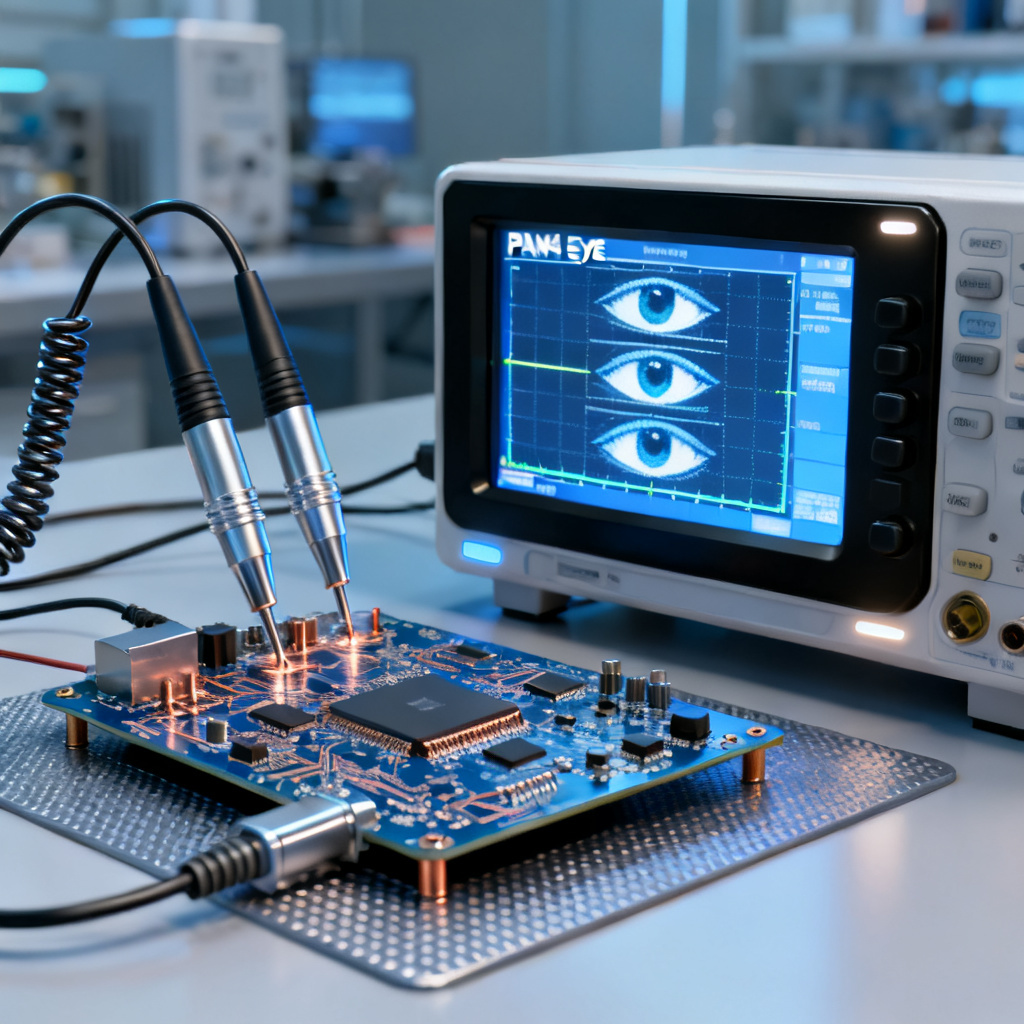
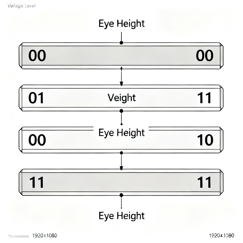
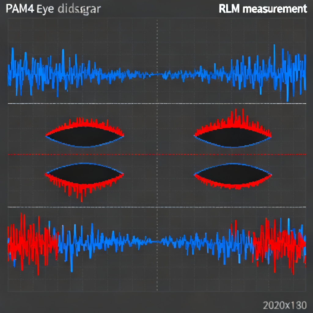
An Eye Diagram PCB for PAM4 signaling is a graphical overlay of multiple bit periods created by sampling a high-speed serial data stream. For PAM4, this overlay produces three distinct eyes, each representing transitions between four voltage levels (00, 01, 10, 11).
This eye diagram reveals signal integrity issues such as noise, jitter, and intersymbol interference (ISI) caused by PCB transmission lines, vias, and connectors. For a PCB manufacturer, a clean eye diagram confirms correct stackup, material selection, and impedance control.
Key parameters measured from an eye diagram include eye height (voltage margin), eye width (timing margin), and jitter. For PAM4, additional metrics like level mismatch (RLM) become essential due to the reduced voltage spacing between levels.
NRZ vs PAM4 Eye Diagram: Core Differences
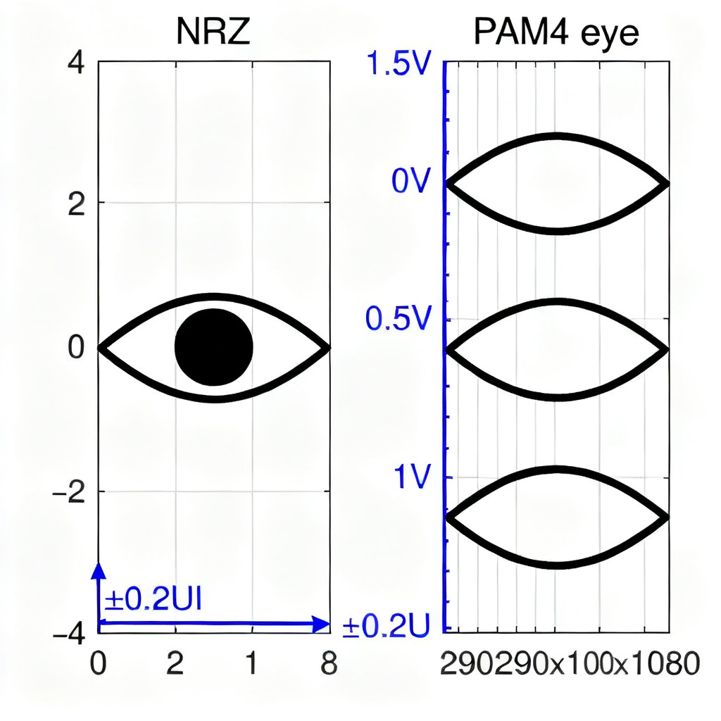
The fundamental difference between NRZ and PAM4 eye diagrams lies in the number of eyes and voltage levels. NRZ uses two levels (0 and 1) producing one open eye, while PAM4 uses four levels producing three stacked eyes.
NRZ Signaling Characteristics
In NRZ signaling, each symbol carries one bit using two voltage levels. The eye diagram shows a single open eye with large vertical margin. NRZ requires double the clock frequency to double data rate, making it bandwidth-inefficient above 28 Gbps.
PAM4 Signaling Characteristics
PAM4 signaling transmits two bits per symbol using four levels, achieving double data rate at the same baud rate. The eye diagram shows three eyes: top, middle, and bottom. The middle eye is the most vulnerable due to smallest voltage margin and highest sensitivity to nonlinearity.
| Parameter | NRZ Eye Diagram | PAM4 Eye Diagram |
|---|---|---|
| Number of Eyes | 1 | 3 |
| Voltage Levels | 2 | 4 |
| Vertical Margin | Large | Small (one-third of NRZ) |
| Jitter Sensitivity | Moderate | High |
| Channel Loss Tolerance | Up to ~20 dB | Up to ~35 dB with equalization |
How to Read a PAM4 Eye Diagram for PCB Design
Reading a PAM4 eye diagram requires analyzing three independent eyes. Each eye provides information about signal quality at different voltage transitions.
The Three Eyes of PAM4
The top eye represents transitions between the highest levels (11 to 10). The middle eye represents transitions between the second-highest and second-lowest levels (10 to 01). The bottom eye represents transitions between the second-lowest and lowest levels (01 to 00).
Critical PAM4 Metrics for High-Speed PCB
Key metrics include eye height per eye, eye width, jitter (random and deterministic), and level mismatch (RLM). RLM measures how evenly the four voltage levels are spaced. Values below 0.95 indicate nonlinearity; below 0.85 is considered failure.
Signal-to-noise ratio (SNR) for PAM4 typically requires >17 dB for a bit error rate of 1e-12, compared to >12 dB for NRZ. This 5 dB penalty makes PAM4 much more sensitive to PCB-induced noise and crosstalk.
PCB Design Considerations for PAM4 Signaling
Designing a PCB for PAM4 signaling requires stricter control over materials, impedance, and layout compared to NRZ. Even small imperfections can close the middle eye and cause bit errors.
Material Selection for PAM4
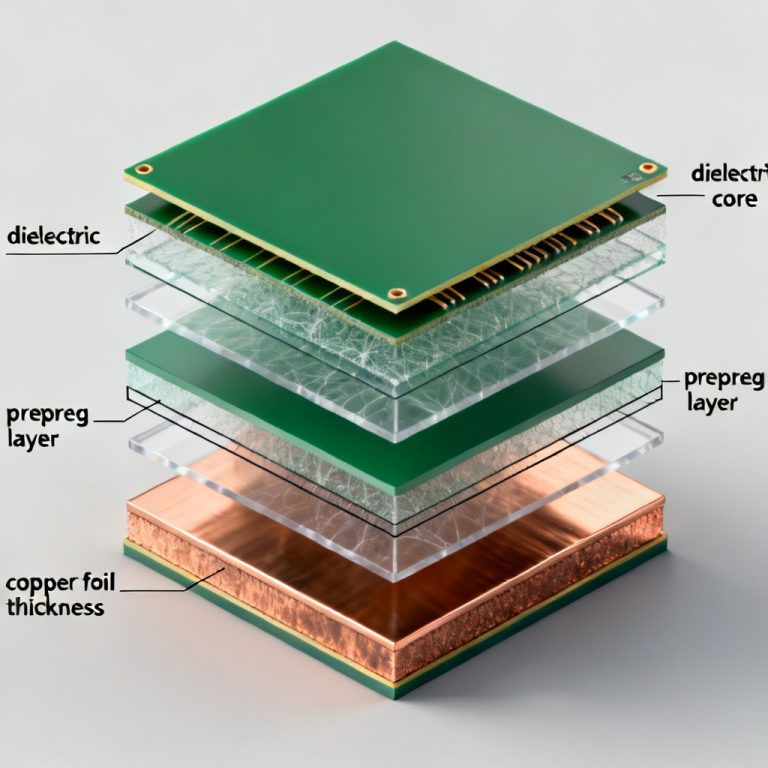
Low-loss laminates with dissipation factor below 0.005 at 10 GHz are mandatory. Standard FR-4 causes excessive eye closure at 28 Gbaud and above. Copper foil roughness must also be minimized to reduce conductor loss.
Impedance Control for PAM4
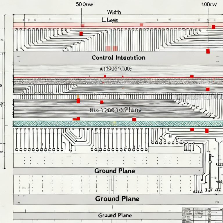
Target impedance tolerance of ±5% is required, tighter than ±10% for NRZ. Impedance mismatches from vias, connector pads, or layer transitions create reflections that distort the eye, especially the middle eye.
Via Design and Backdrilling
Backdrilled or microvia transitions minimize stub length. Via stubs longer than 10 mils at 28 Gbaud create resonant notches in insertion loss, destroying eye opening. Stitching vias along ground planes reduce return path discontinuities.
Crosstalk Management
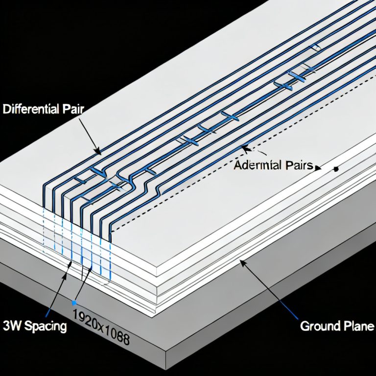
Maintain minimum 3W spacing between PAM4 traces. Use ground stitching vias to reduce coupling. Even -30 dB of crosstalk can cause bit errors in PAM4 due to reduced voltage margin.
Practical Tips for Testing PAM4 Eye Diagrams on PCBs
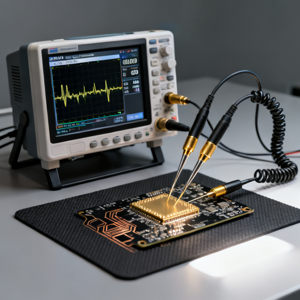
Testing PAM4 eye diagrams requires specialized equipment and methodology. Use a real-time oscilloscope with PAM4 analysis software and clock recovery. Measure at the BGA pad using a high-bandwidth probe to avoid test fixture effects.
Check all three eyes independently. The middle eye is the weakest link. Calculate RLM using the scope’s built-in measurement. Compare to NRZ baseline at half-rate to isolate noise or nonlinearity issues.
Frequently Asked Questions About Eye Diagram PCB for PAM4 Signaling
What is the main difference between NRZ and PAM4 eye diagrams?
The main difference is that NRZ produces one open eye while PAM4 produces three stacked eyes due to four voltage levels. PAM4 achieves double data rate at same baud rate but with reduced voltage margin.
Why is the middle eye in PAM4 most vulnerable?
The middle eye has the smallest voltage margin because it sits between the second-highest and second-lowest levels. It is most affected by nonlinearities and noise, making it the first to close under poor PCB design.
What PCB materials are required for PAM4 signaling?
Low-loss laminates with Df below 0.005 at 10 GHz are required. Materials like Megtron 6 or Rogers 4350B are common. Standard FR-4 causes excessive loss and eye closure at 28 Gbaud.
How does impedance control affect PAM4 eye diagrams?
Tighter impedance tolerance (±5%) is needed for PAM4 compared to NRZ (±10%). Impedance mismatches create reflections that distort the eye, particularly the middle eye, increasing bit error rate.
What is RLM in PAM4 eye diagrams?
RLM (Level Mismatch) measures how evenly the four voltage levels are spaced. Values below 0.95 indicate nonlinearity; below 0.85 is considered failure. Poor RLM closes the middle eye and increases BER.
Conclusion: Why Your PCB Supplier Must Understand PAM4
The transition from NRZ to PAM4 is a hardware revolution. A PCB designed for NRZ will fail for PAM4 due to tighter requirements on materials, impedance, and layout. Ensure your PCB manufacturer provides low-loss stackups, backdrilling, microvia fabrication, and signal integrity simulation reports including PAM4 eye diagrams.
At [Your Company Name], we specialize in high-speed PCB fabrication for 56 Gbps and 112 Gbps PAM4 applications. Our advanced simulation tools and manufacturing processes ensure your eye diagrams remain open, your RLM stays above 0.95, and your data rates reach the next generation.