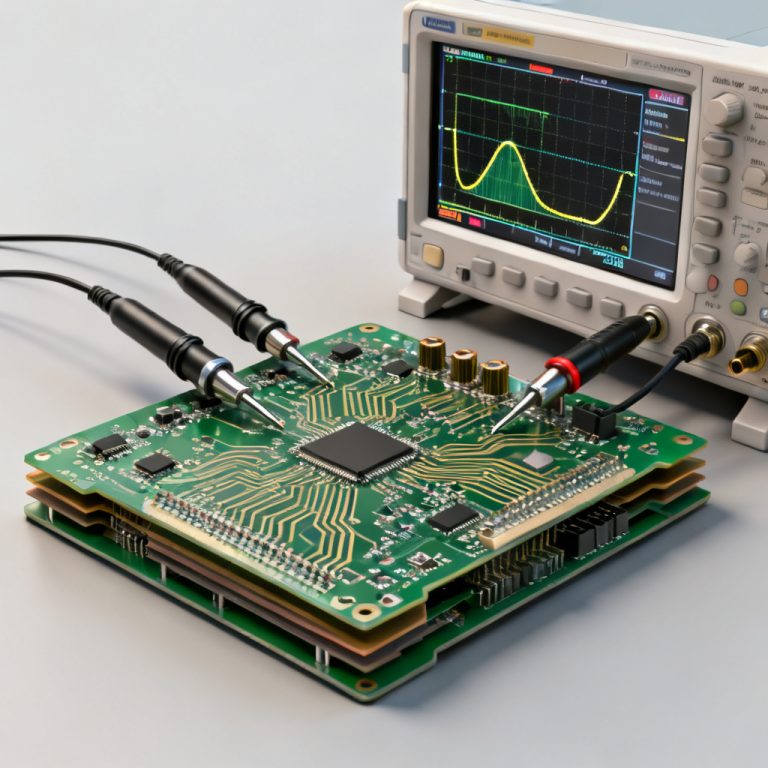
Eye Diagram PCB Mask Testing is a critical signal integrity validation method for high-speed PCB design, ensuring your boards meet stringent pass/fail criteria for reliable data transmission. This comprehensive guide explains the fundamentals, pass/fail boundaries, and industry standards.
What Is Eye Diagram PCB Mask Testing?
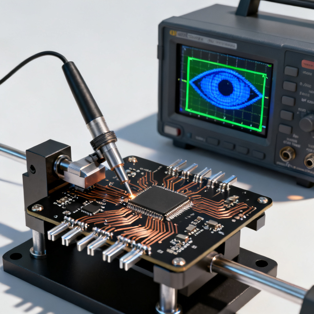
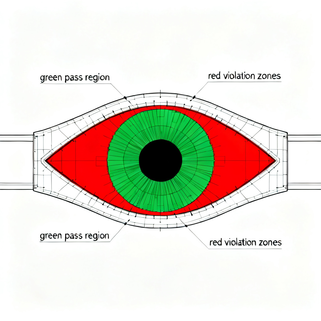
Eye Diagram PCB Mask Testing evaluates signal quality by comparing a measured eye diagram against a predefined mask—geometric boundaries in the voltage-time domain. The mask defines the minimum acceptable eye opening for interfaces like PCIe, USB, HDMI, and DDR. A pass occurs when the entire eye diagram remains outside the mask region; a fail happens when any part intrudes into the forbidden zone.
Key Components of an Eye Diagram
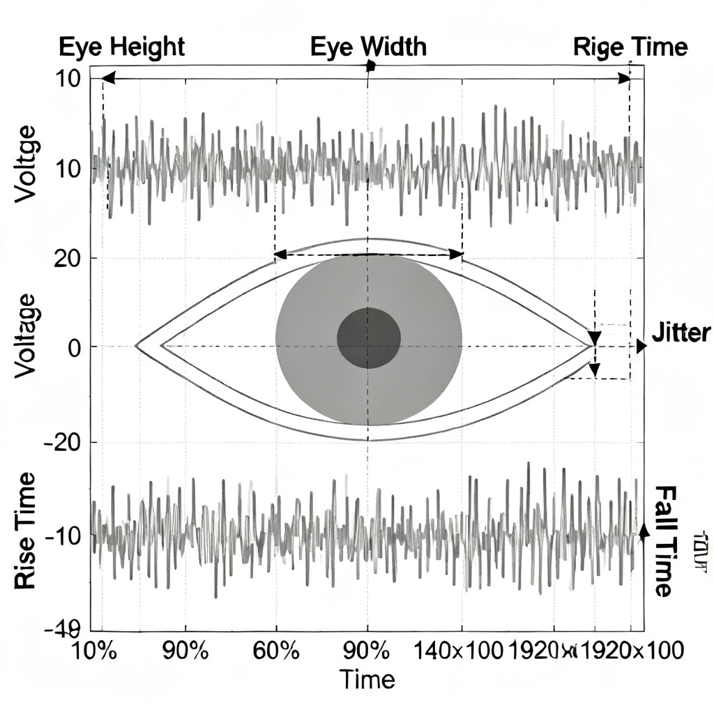
- Eye Height (Vertical Opening): Difference between highest and lowest voltage levels at the sampling point. Larger height indicates better noise immunity.
- Eye Width (Horizontal Opening): Time interval during which the signal is stable. Wider width means better timing margin.
- Jitter: Deviation from ideal timing, visible as horizontal thickening at crossing points.
- Rise/Fall Times: Transition slopes; slower edges can close the eye.
- Overshoot/Undershoot: Voltage excursions beyond nominal levels, potentially damaging receivers.
Pass/Fail Criteria Explained
The pass/fail criteria for Eye Diagram PCB Mask Testing derive from bit error rate (BER) requirements. For example, PCIe Gen 4 requires BER less than 10⁻¹². The mask ensures minimum voltage and timing margins to achieve this BER.
Eye Height Pass/Fail Criteria
Minimum Eye Height is specified in millivolts (mV). For USB 3.2, the minimum is 100 mV at the receiver. Failure causes include excessive noise, ground bounce, or insufficient voltage swing due to lossy PCB materials.
Eye Width Pass/Fail Criteria
Minimum Eye Width is specified in picoseconds (ps) or as a fraction of the unit interval (UI). For PCIe Gen 5 (32 GT/s), the minimum is 0.3 UI (approx. 9.375 ps). Failure causes include jitter from clock recovery, crosstalk, or intersymbol interference (ISI).
Mask Margin
Mask margin is the distance between the measured eye diagram and mask boundaries. A positive margin (e.g., +10% eye height) indicates a robust design. Many standards require 10–20% margin to account for manufacturing tolerances and temperature variations.
Violation Zones
- Center of the Eye: Most critical zone. Any signal here indicates timing or voltage violation.
- Corners of the Mask: Violations suggest excessive overshoot/undershoot from impedance mismatches.
- Edge of the Eye: Thickening or closure suggests high jitter or slow rise/fall times.
BER-Based Pass/Fail
Some standards (e.g., 100G Ethernet) use a BER contour. The eye diagram must achieve a specific BER (e.g., 10⁻¹²) at mask boundaries. A design passing the mask may still fail if BER contour shows excessive error probability.
Industry Standards and Their Mask Requirements
| Standard | Data Rate | Minimum Eye Height | Minimum Eye Width | Mask Shape |
|---|---|---|---|---|
| PCIe Gen 4 | 16 GT/s | 175 mV (differential) | 0.3 UI | Hexagonal |
| PCIe Gen 5 | 32 GT/s | 100 mV (differential) | 0.3 UI | Hexagonal |
| USB 3.2 | 10 Gbps | 100 mV (differential) | 0.4 UI | Octagonal |
| HDMI 2.1 | 12 Gbps per lane | 150 mV (single-ended) | 0.3 UI | Custom (FRL) |
| 10G Ethernet (SFP+) | 10.3125 Gbps | 50 mV (differential) | 0.4 UI | Rectangular (IEEE 802.3) |
| DDR4 | 3200 MT/s | 150 mV (single-ended) | 0.5 UI | Diamond-shaped (JEDEC) |
How to Perform Eye Diagram Mask Testing on a PCB
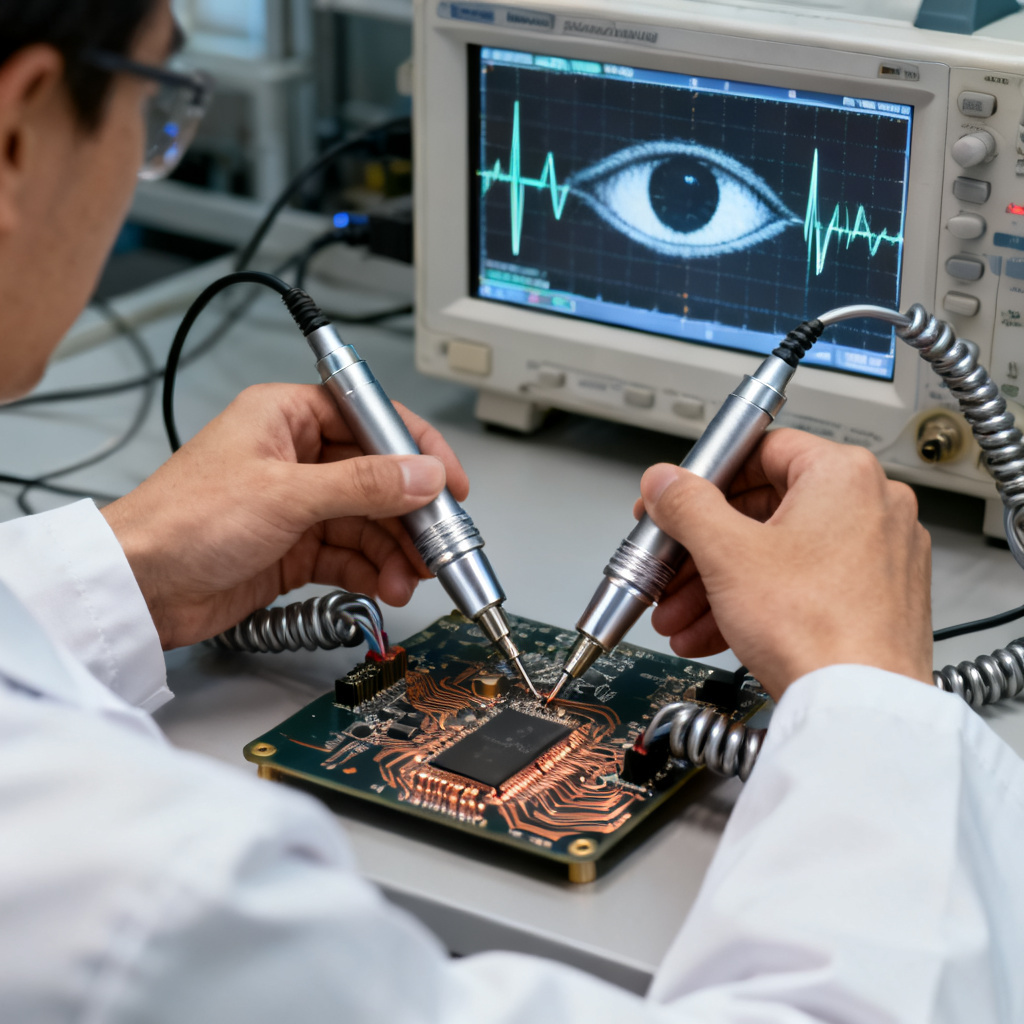
Performing Eye Diagram PCB Mask Testing requires a high-bandwidth oscilloscope (≥4× data rate), differential probes, and a PRBS pattern. Follow these steps:
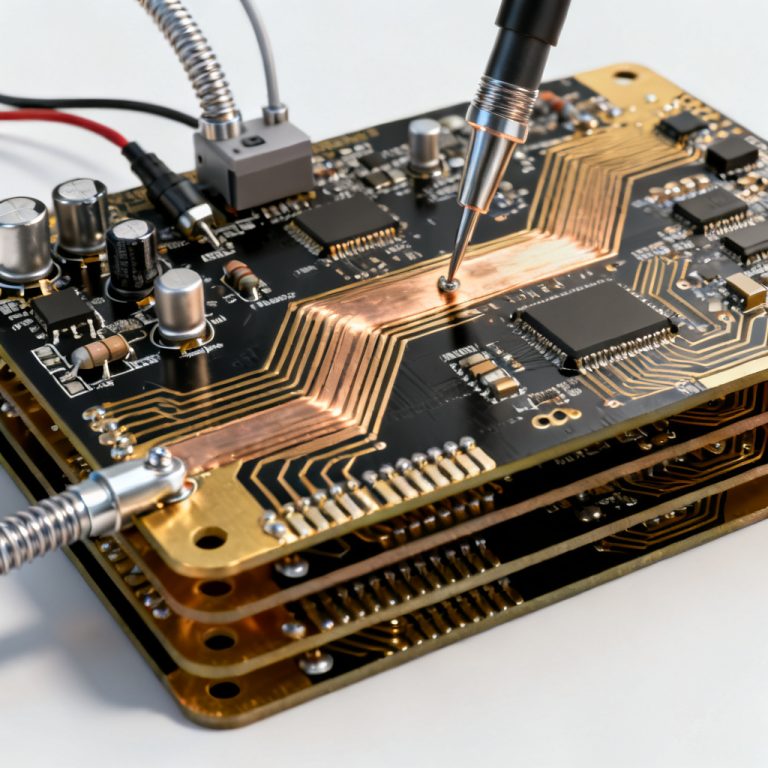
- Set Up Test Environment: Connect probes to PCB test points at the receiver end. Ensure DUT transmits a PRBS pattern.
- Configure Oscilloscope: Set clock recovery with standard PLL bandwidth. Adjust timebase to show 1–2 UI per division. Enable persistence for thousands of bits.
- Load Standard Mask: Use built-in mask libraries for PCIe, USB, HDMI, or manually input coordinates from the standard.
- Acquire and Analyze: Capture eye diagram over 10⁶ bits. Run mask test; oscilloscope highlights violations in red.
- Interpret Results: Pass = no violations. Fail = one or more violations; note location and margin depth.
Common Pitfalls
- Probe Loading: Poor grounding or excessive capacitive loading distorts the eye.
- Incorrect Clock Recovery: Wrong PLL bandwidth shifts eye position.
- Pattern Dependency: PRBS7 vs PRBS31 produces different jitter levels. Use pattern specified by standard.
Troubleshooting Failed Mask Tests
If your high-speed PCB fails an eye diagram mask test, investigate these root causes:
PCB Material and Stackup
High-loss materials like FR-4 at frequencies >5 GHz cause attenuation, closing the eye. Use low-loss materials (e.g., Rogers 4350B, Megtron 6) and optimize stackup for controlled impedance (50Ω single-ended, 100Ω differential).
Trace Routing and Vias
Long traces (>10 inches), multiple vias, or stubs create reflections and ISI. Minimize trace lengths, use back-drilling for vias, and avoid 90° corners (use 45° or curved traces).
Power Integrity
Power supply noise from switching regulators modulates the signal, reducing eye height. Add decoupling capacitors (0.1 µF and 1 µF) near transmitter/receiver, and use a clean power plane.
Connector and Cable Effects
Poor connector mating or lossy cables introduce additional jitter. Use high-speed connectors (Samtec, Molex) with low insertion loss and ensure impedance matching.
Clock Recovery Issues
A weak or noisy clock signal can misalign the eye. Verify clock source and use a dedicated clock recovery module if needed.
Advanced Topics: Beyond Basic Pass/Fail
Statistical Eye Analysis (SEA)
SEA uses a BER contour to predict eye opening at a specific BER (e.g., 10⁻¹²). This is more accurate for high-speed links where jitter is non-Gaussian.
Channel Operating Margin (COM)
Used in IEEE standards (e.g., 100G-KR), COM combines eye diagram with channel loss and crosstalk. A COM > 3 dB is generally required.
Pre-Emphasis and Equalization
Many high-speed transmitters use pre-emphasis (boosting high frequencies) or DFE (decision feedback equalization) to open the eye. Mask testing should be performed with equalization enabled as per the standard.
Why Partner with a High-Speed PCB Manufacturer for Mask Testing?
As a B2B buyer, you need a partner who validates signal integrity. Look for in-house testing capability (50+ GHz oscilloscope), standard compliance (PCIe, USB, HDMI, Ethernet), data-driven reports with eye diagram screenshots and pass/fail certificates, and design support (SI simulation using Ansys HFSS or ADS).
At [Your Company Name], we specialize in high-speed PCB manufacturing with a dedicated signal integrity lab. Every board for 10+ Gbps applications undergoes rigorous Eye Diagram PCB Mask Testing. Our engineers optimize your design for first-pass success.
FAQ: Eye Diagram PCB Mask Testing
What is the main purpose of Eye Diagram PCB Mask Testing?
The main purpose is to validate that a high-speed PCB meets signal integrity requirements by comparing the eye diagram against a mask, ensuring reliable data transmission at specified BER.
How do I interpret a failed eye diagram mask test?
A failure indicates that the signal violates voltage or timing margins. Common causes include lossy materials, poor routing, power integrity issues, or connector problems. Investigate using the troubleshooting guide above.
What standards require Eye Diagram PCB Mask Testing?
Standards like PCIe Gen 4/5, USB 3.2, HDMI 2.1, 10G Ethernet, and DDR4 specify mask testing requirements. Each defines minimum eye height, eye width, and mask shape.
Can I perform Eye Diagram PCB Mask Testing without an oscilloscope?
No, a high-bandwidth oscilloscope (≥4× data rate) with clock recovery and mask testing software is required. For accurate results, use a scope with built-in mask libraries.
What is the difference between mask margin and eye opening?
Mask margin is the distance between the measured eye and mask boundaries, while eye opening is the actual voltage/timing window. Positive margin means the eye opening exceeds the minimum requirement.
Conclusion: The Bottom Line on Eye Diagram Mask Testing
Eye Diagram PCB Mask Testing is a critical quality assurance step ensuring your high-speed PCB functions reliably. Understanding pass/fail criteria—eye height, eye width, mask margin, and BER requirements—enables informed decisions about design, materials, and manufacturing partners. Key takeaways: a passing eye diagram guarantees minimum margins; failures trace to lossy materials, routing, or power integrity; always request mask test reports with margin data; for cutting-edge speeds, use statistical eye analysis.
Ready to ensure your next high-speed PCB design passes? Contact us today for a free design review and mask testing consultation.