In high-speed PCB design, the eye mask in eye diagram PCB is a critical pass/fail tool for signal integrity. This guide explains how to interpret and apply eye mask limits to ensure reliable custom PCB fabrication.
What Is an Eye Mask in Eye Diagram PCB?
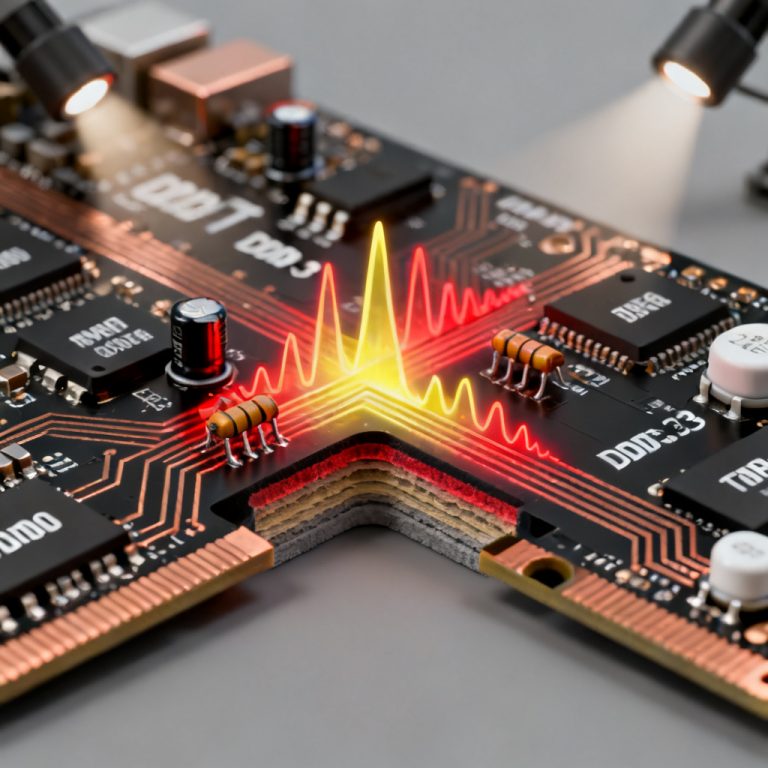
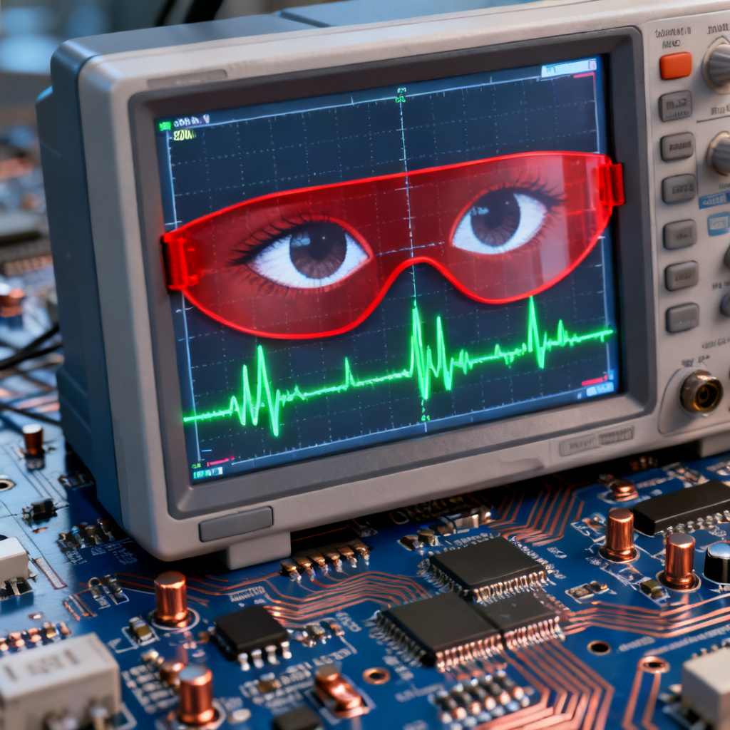
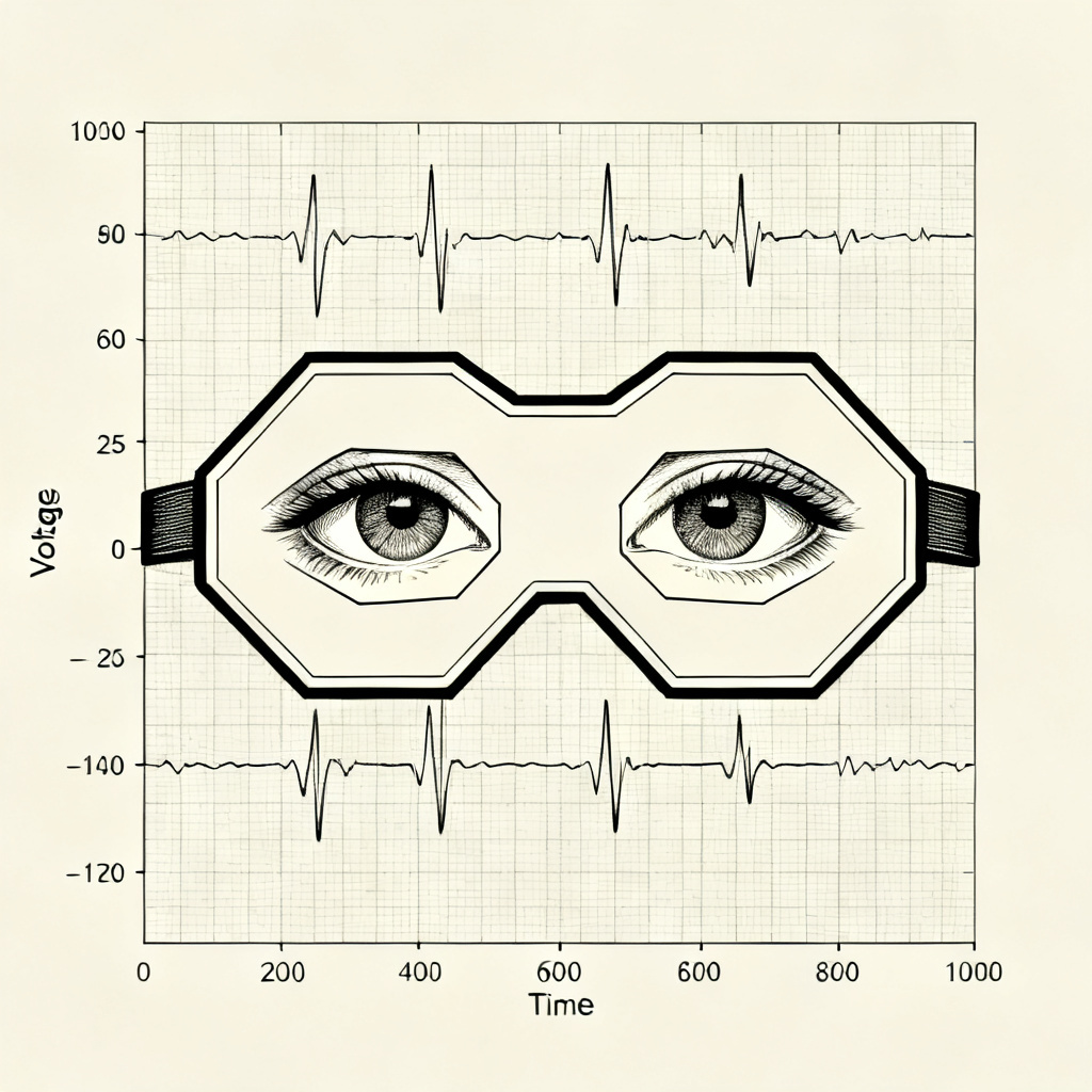
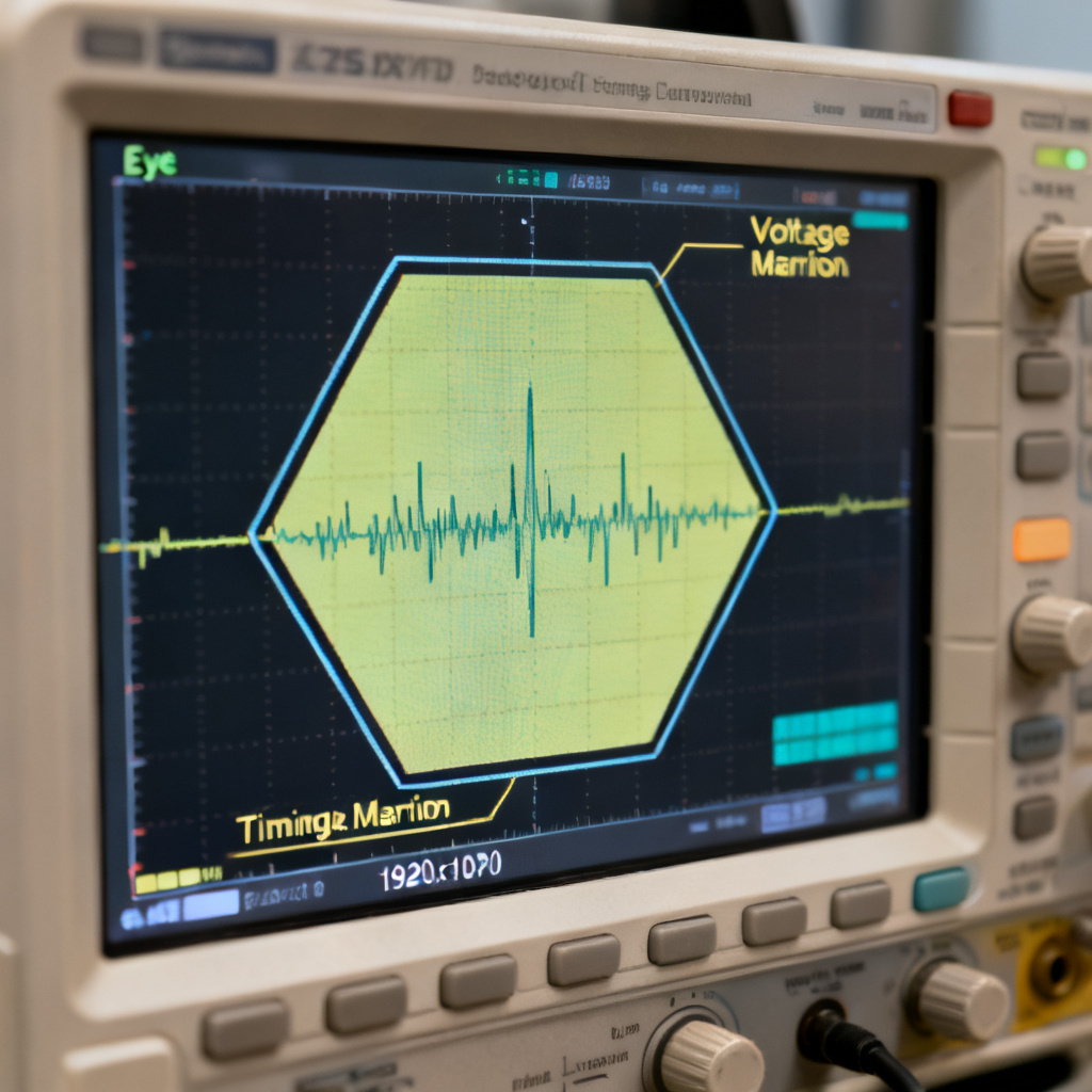
An eye mask in eye diagram PCB is a predefined geometric shape overlaid on an eye diagram. It defines forbidden zones where the signal waveform must never enter. If any portion of the signal touches or crosses the mask region, the design fails the test.
Key characteristics of an eye mask include its location—centered around the eye opening—and its shape, typically a hexagon or multi-segment polygon. Dimensions are defined by standards like PCIe, USB, Ethernet, or DDR. The purpose is to guarantee sufficient voltage margin and timing margin for correct receiver sampling.
For B2B PCB buyers, the eye mask provides an objective, repeatable pass/fail criterion. Without it, you only have a qualitative view of the eye. This ensures your design works in the target system, reducing re-spin and field failure risks.
How to Interpret the Eye Mask in Eye Diagram PCB
Interpreting an eye mask in eye diagram PCB requires understanding three key regions:
Vertical Eye Opening (Voltage Margin)
The mask’s top and bottom boundaries define minimum and maximum voltage levels. This ensures the receiver can distinguish logic ‘1’ from logic ‘0’ with noise immunity. A violation indicates insufficient amplitude due to loss, reflections, or crosstalk.
Horizontal Eye Opening (Timing Margin)
The left and right boundaries define the minimum time window (unit interval) during which the signal must be stable. This accounts for jitter—random or deterministic timing variations. A violation means signal transitions cause setup/hold time failures.
Mask Corner Regions (The Diamond or Hexagon)
The diagonal edges represent combined voltage and timing tolerance. This is the most stringent region, catching signals simultaneously marginal in both voltage and timing. A signal passing vertical and horizontal limits individually might still fail the corner region.
Practical interpretation: Look for a clean, open eye passing well clear of mask edges. Touching the mask indicates marginal failure due to process variation or temperature. Crossing the mask is a clear failure requiring design correction.
How to Apply Eye Mask Limits in PCB Design and Testing
Applying eye mask in eye diagram PCB limits involves two phases: design simulation and production testing.
Phase 1: Design Simulation (Pre-Production)
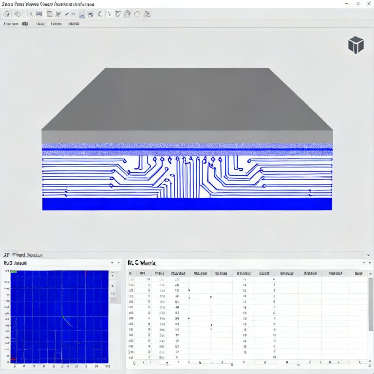
Use simulation tools like HyperLynx, ADS, or SIwave to generate eye diagrams from your PCB stackup. Apply the relevant eye mask from chipset datasheets or standards. Best practices include using a derated mask with 10-20% margin on dimensions, checking at multiple corners (worst-case temperature, voltage, process), and focusing on the worst-case channel for multi-gigabit designs.
Phase 2: Production Testing (Post-Fabrication)
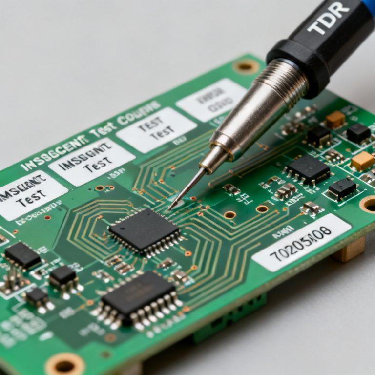
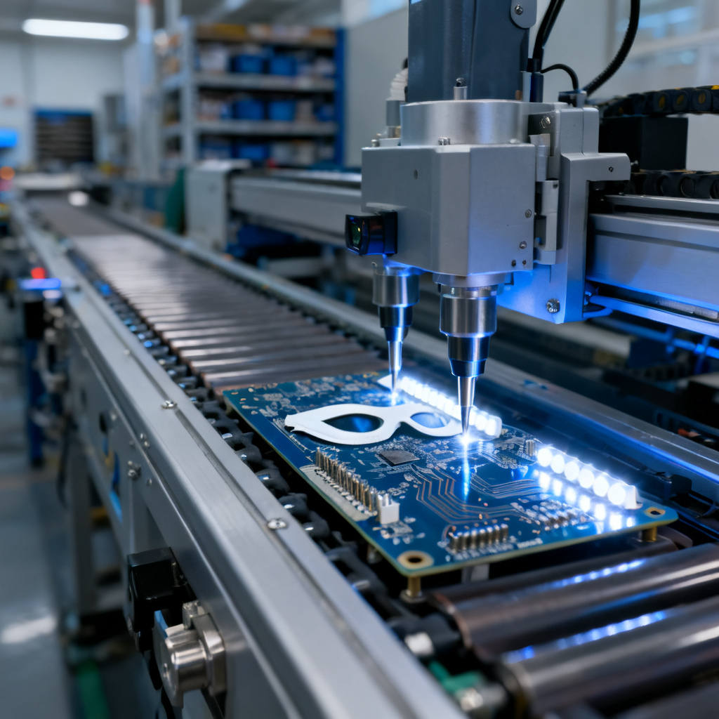
In manufacturing, we use automated test equipment or high-bandwidth oscilloscopes with eye mask testing software. The process involves setting the mask (loading standard mask files like .msk or .eym), configuring the test (e.g., 100% of boards, 10,000 transitions per channel), running pass/fail tests, and recording results including margin to failure and hit count.
Critical note for B2B buyers: Always request eye mask margin data in your PCB test report. A passing result with 30% margin indicates robust manufacturability.
Common Eye Mask Standards and Limits
Different high-speed interfaces have unique eye mask requirements. The following table summarizes common standards tested in eye mask in eye diagram PCB analysis:
| Interface | Data Rate | Mask Shape | Typical Vertical Limit | Typical Horizontal Limit |
|---|---|---|---|---|
| PCIe Gen4 | 16 GT/s | Hexagon | 100 mV | 0.3 UI |
| USB 3.2 Gen2 | 10 Gbps | Hexagon | 100 mV | 0.3 UI |
| 10GBASE-KR | 10.3125 Gbps | Hexagon | 100 mV | 0.2 UI |
| DDR4/5 | Up to 6.4 Gbps | Rectangular | 150-200 mV | 0.2-0.3 UI |
| SATA 3.0 | 6 Gbps | Hexagon | 120 mV | 0.3 UI |
These limits apply to the receiver input after the channel. The transmitter output typically has a wider, cleaner eye. The mask at the receiver accounts for channel loss, ISI, and crosstalk.
Common Eye Mask Violations and How to Fix Them
Even with careful design, eye mask in eye diagram PCB failures can occur. The table below lists frequent causes and solutions:
| Violation Type | Likely Cause | Fix in Design/Layout |
|---|---|---|
| Vertical closure (eye height too small) | Excessive trace loss | Use lower-loss materials (Rogers, Megtron); shorten trace length; use thicker copper; add pre-emphasis/de-emphasis. |
| Horizontal closure (eye width too small) | Excessive jitter | Improve clock recovery; reduce crosstalk (increase spacing, add shielding); use low-jitter oscillator; add equalization (CTLE, DFE). |
| Mask corner violation | Combined loss and jitter | Simultaneously optimize loss (material, length) and jitter (routing, termination, power integrity). |
| Asymmetric mask violation | Impedance mismatch (stub, via, connector) | Ensure 50Ω or 100Ω differential impedance; optimize via back-drilling; use matched-length routing. |
Pro tip: For high-speed PCBs, via stubs are the #1 cause of asymmetric eye mask failures. Always request back-drilled vias for signals above 10 Gbps.
Why Trust Our High-Speed PCB Manufacturing
As your B2B partner for high-speed PCB fabrication, we go beyond basic manufacturing. Our process includes full eye mask in eye diagram PCB testing for every high-speed channel on every production board. We provide compliance testing against PCIe, USB, Ethernet, and DDR standards, along with Design for Manufacturing (DFM) feedback to optimize your stackup and routing for better eye mask margins.
We offer material selection guidance to match your target data rate—FR-4 for below 5 Gbps, high-speed laminates for above 10 Gbps. Every board we ship includes a passing eye mask test report with margin data, ensuring your design works reliably in the field.