In high-speed digital design, every signal is a transmission line. For a signal to propagate correctly, it must have a continuous, low-inductance return path directly adjacent to its trace. This is not just a theoretical nicety—it is a fundamental requirement for signal integrity (SI) and electromagnetic compatibility (EMC). When designing for Ball Grid Array (BGA) escape routing and dense routing areas, maintaining this return path becomes the single most critical challenge.
A broken or poorly managed return path leads to:
- Increased loop inductance, causing signal degradation and ringing.
- Common-mode noise, which radiates as EMI.
- Simultaneous Switching Noise (SSN), affecting power integrity.
- Crosstalk between adjacent signals.
This pillar page will guide you through the best practices, industry-proven strategies, and advanced techniques for managing return path specifically in BGA escape regions and high-density routing corridors. By the end, you will understand how to design PCBs that perform reliably at high speeds.
Chapter 1: The Fundamentals of Return Current Path in High-Speed PCB
1.1 The Physics of Return Current
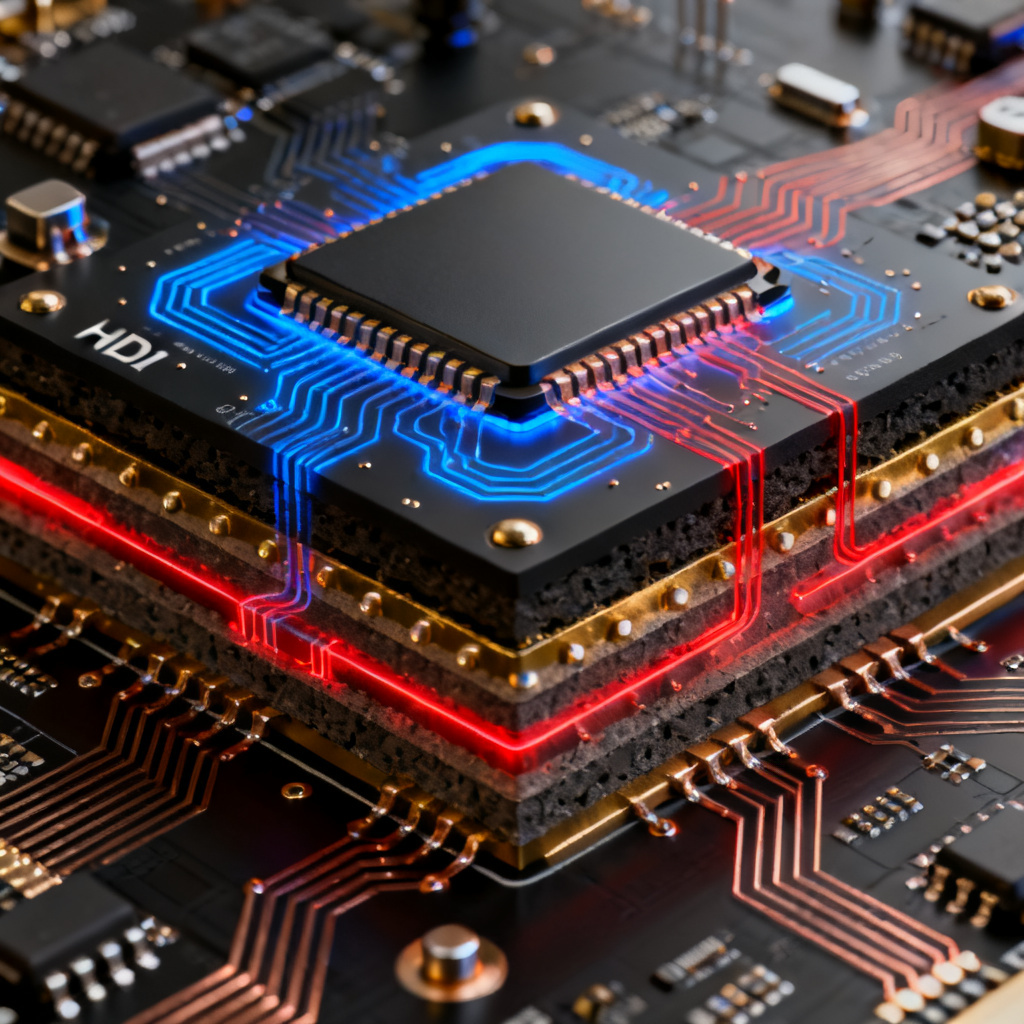
At low frequencies, return current follows the path of least resistance (DC path), typically through the ground plane. However, at high frequencies (above approximately 1 MHz), the return path current follows the path of least inductance—directly under the signal trace, on the adjacent reference plane.
Key Principle: The return current flows directly beneath the signal trace, on the plane that is closest to the trace layer. The distance between the signal trace and its reference plane determines the characteristic impedance and the loop area.
1.2 Why the Return Path is Critical for BGA Escape
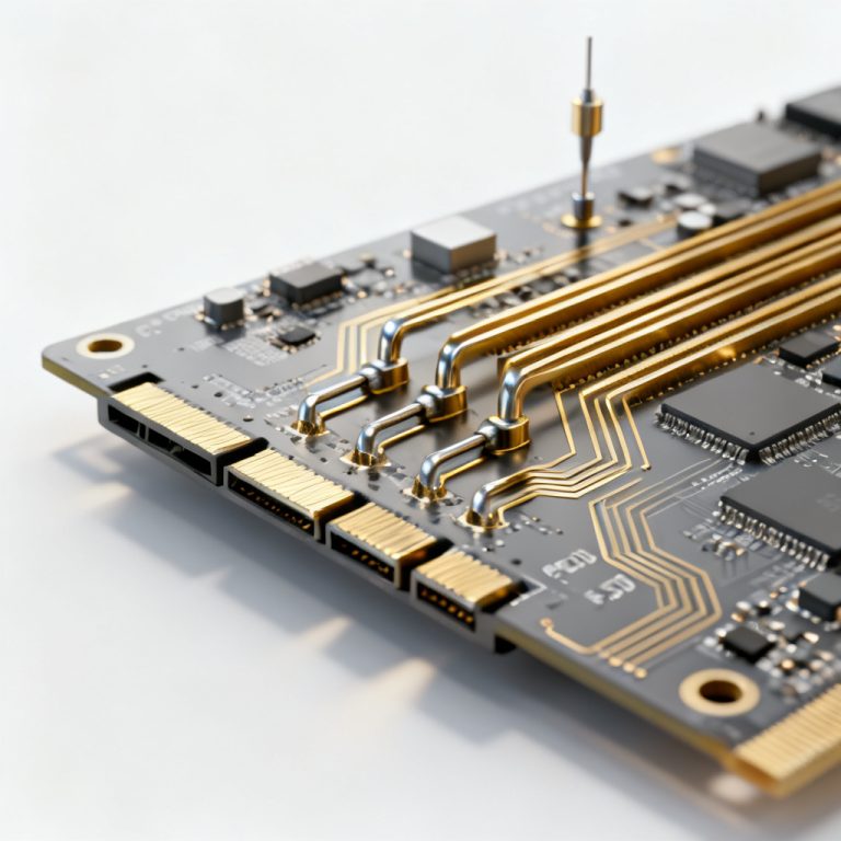
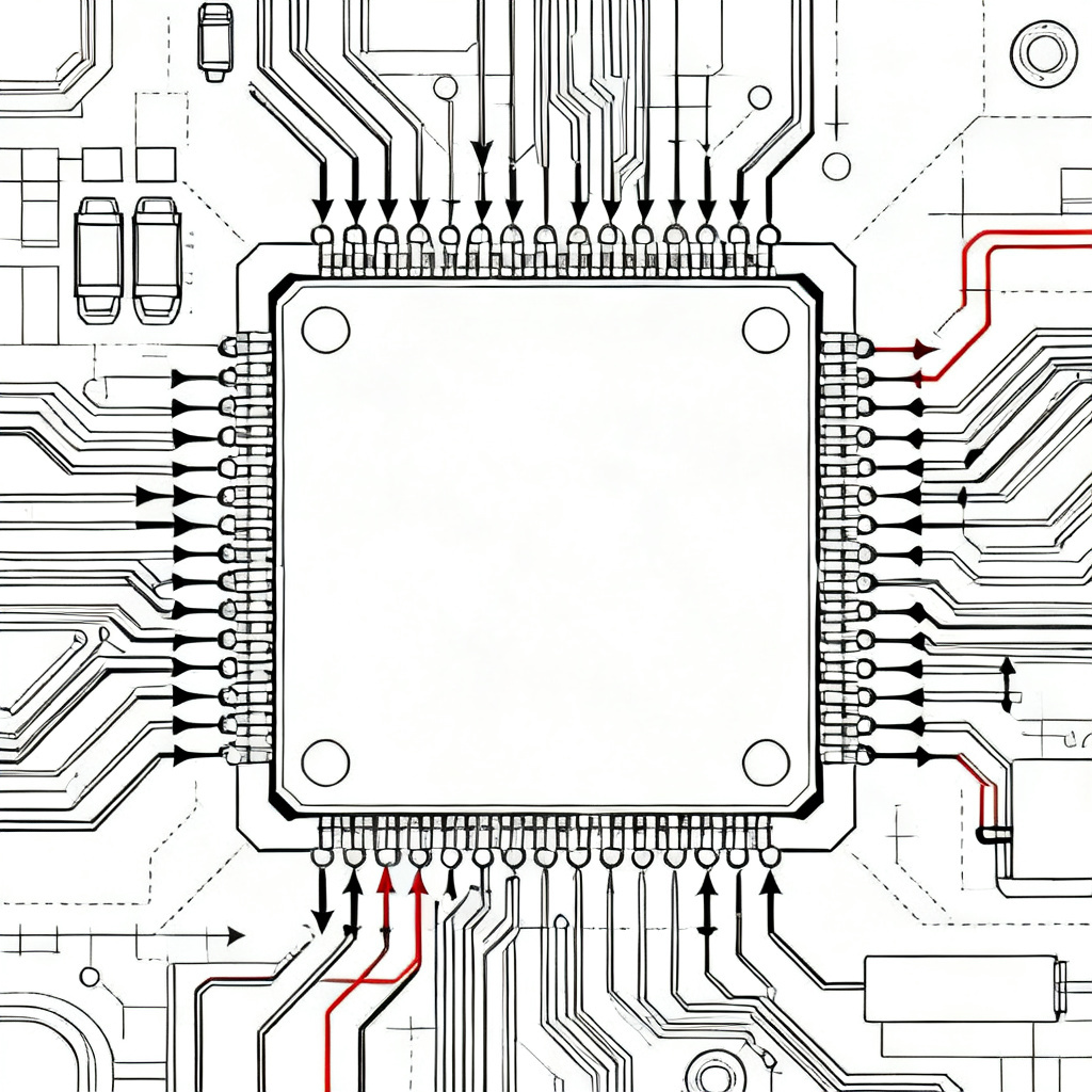
In BGA escape routing, traces are often forced to change layers (via transitions) to fan out from the dense ball field. Each time a signal changes layers, its return current must also change reference planes. If the return path is interrupted—for example, if the vias for the signal and its reference plane are not properly paired—the return current must find an alternative, inductive path. This creates a large current loop, degrading signal quality.
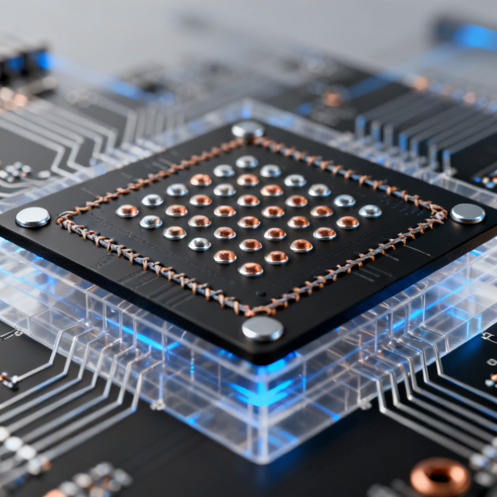
The BGA Problem: The BGA area is a “starvation zone” for ground and power vias. There are simply too many signals and too few available via locations within the ball grid array. This forces designers to make compromises that can ruin high-speed performance.
Chapter 2: BGA Escape Routing Strategies for Return Path Integrity
2.1 The Dog-Bone and Via-in-Pad Techniques
There are two primary methods for escaping traces from a BGA:
- Dog-Bone Fanout: A short trace runs from the BGA ball to a via placed outside the ball array. This is the most common method but consumes routing channels.
- Via-in-Pad (VIP): A via is placed directly on the BGA pad. This saves space but requires filling and plating (e.g., conductive epoxy or copper-filled vias) to prevent solder wicking. VIP is often necessary for ultra-fine pitch BGAs (0.5mm or less).
Return Path Implication: In dog-bone routing, the trace from the ball to the via is on the top layer. The return current must flow from the top-layer ground plane to the inner-layer ground plane through a ground via. If no ground via is nearby, the return path is broken.
Best Practice: For every signal via in a BGA escape, place a ground via as close as possible (ideally within 1 mm or less). This creates a coaxial-like structure for the transition, minimizing loop inductance.
2.2 Layer Stack-Up Planning for BGA Escape
The stack-up must be designed to support BGA escape before routing begins. A typical high-speed BGA stack-up includes:
- Top Layer: Signal layer for BGA escape (short traces).
- Layer 2: Ground plane (continuous, no splits).
- Layer 3: Power plane (or secondary ground).
- Layer 4: Signal layer for horizontal routing.
- Layer 5: Ground plane.
- Layer 6: Signal layer for vertical routing.
- Bottom Layer: Signal or ground.
Critical Rule: The reference planes must be continuous under the BGA. Avoid splitting ground or power planes in the BGA area. If a split is unavoidable (e.g., for mixed-signal designs), the gap must be bridged with stitching capacitors or by routing signals over the gap only on layers where the return path can be maintained.
2.3 Via Stitching and Shielding
In dense BGA areas, you cannot place a ground via for every signal via. Instead, use via stitching:
- Place ground vias at the corners of each BGA quadrant.
- Use a grid of ground vias in the BGA area—typically one ground via for every four to eight signal vias.
- For critical differential pairs (e.g., PCIe, USB, HDMI), place a ground via on either side of the pair at the point of layer transition.
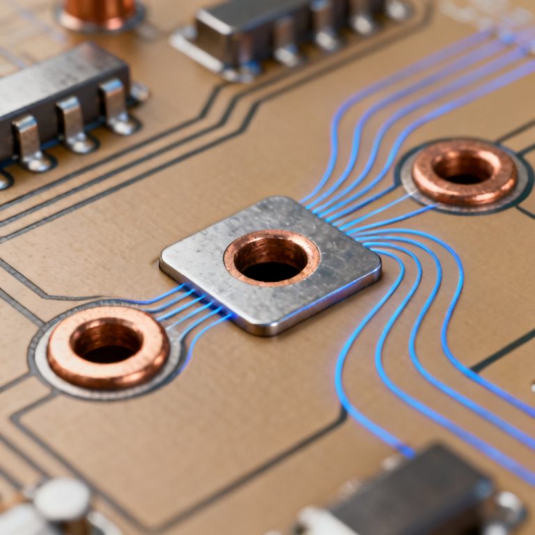
Advanced Technique: For extremely high-speed signals (e.g., 25 Gbps and above), consider using coaxial via structures where a signal via is surrounded by a fence of ground vias. This provides the lowest possible return path inductance.
Chapter 3: Managing Return Paths in Dense Routing Areas
3.1 The Problem of Plane Discontinuities
Dense routing areas are often characterized by multiple signal layers, numerous vias, and power plane splits. When a trace passes over a split in its reference plane, the return current must detour around the split. This increases loop area, causing:
- Impedance discontinuity (the characteristic impedance changes at the split).
- EMI radiation (the loop acts as an antenna).
- Crosstalk (the return current from one signal couples into another).
The Rule: Never route a high-speed signal over a split in its reference plane. If a split is unavoidable, use a stitching capacitor (typically 100 nF to 10 µF) across the split near the crossing point. The capacitor provides a low-impedance path for the return current at high frequencies.
3.2 Stitching Capacitors for Plane Crossings
When a signal must cross from one power domain to another (e.g., from a 3.3V plane to a 1.8V plane), the return path is interrupted. A stitching capacitor bridges the gap:
- Place the capacitor as close as possible to the signal via.
- Use multiple capacitors in parallel to reduce ESL (Equivalent Series Inductance).
- For differential pairs, place two capacitors (one for each signal) or one capacitor for the pair if space is tight.
Limitation: Stitching capacitors are only effective up to a few GHz. At millimeter-wave frequencies (e.g., 28 GHz for 5G), even a small capacitor has too much inductance. In such cases, avoid plane splits entirely.
3.3 Ground Via Fencing for Isolation
In dense routing areas, signals can couple through the substrate (substrate crosstalk). A via fence (also called a picket fence) is a row of ground vias placed between two routing channels or between a signal and a noisy area (e.g., a switching regulator).
- Spacing between vias should be less than λ/20 (where λ is the wavelength of the highest frequency component).
- For typical high-speed digital (e.g., 1-10 GHz), via spacing of 1-2 mm is sufficient.
- The fence acts as a waveguide below cutoff, preventing electromagnetic fields from leaking between regions.

Chapter 4: Advanced Techniques for High-Speed BGA and Dense Routing
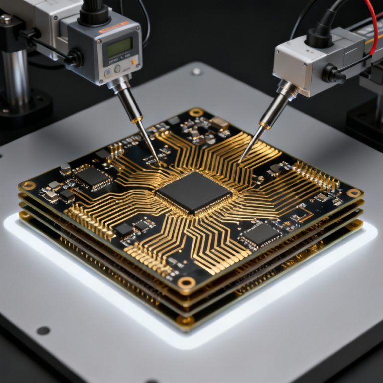
4.1 Microvia and HDI (High-Density Interconnect) Technology
For ultra-fine pitch BGAs (0.4mm or less), standard through-hole vias are too large. HDI technology uses:
- Microvias: Laser-drilled vias with diameters of 100-150 µm.
- Blind and Buried Vias: Vias that connect only specific layers, reducing via stub effects.
- Stacked Microvias: Microvias placed directly on top of each other to create a vertical interconnect.
Return Path Advantage: HDI allows placing ground microvias directly under BGA balls, providing an extremely short return path. This is essential for DDR5, GDDR6, and high-speed SERDES interfaces.
4.2 Via Stub Management
A via stub is the unused portion of a through-hole via that extends beyond the signal layer to the bottom of the board. At high frequencies, the stub acts as a resonant cavity, causing insertion loss and reflections.
Solutions:
- Back-drilling: Remove the unused portion of the via after plating. This is standard for signals above 10 Gbps.
- Use blind or buried vias: Eliminate stubs entirely.
- Via-in-pad with back-drilling: Combine VIP with back-drilling for the lowest possible via inductance.
4.3 Differential Pair Routing in Dense Areas
Differential pairs are less sensitive to return path discontinuities because the return current is the difference between the two signals. However, they are not immune:
- Keep the pair tightly coupled (edge-to-edge spacing equal to the dielectric thickness).
- Avoid crossing plane splits—even differential pairs suffer from common-mode conversion at discontinuities.
- Use ground vias at the point of layer transition for each pair.
BGA Escape for Differential Pairs: When escaping differential pairs from a BGA, route the two signals on the same layer and transition to inner layers together. Place a ground via between the two vias of the pair if possible.
Chapter 5: Practical Design Rules and Checklist
5.1 Return Path Design Rules
- Rule 1: Every signal via must have a ground via within 1.5 mm (60 mils) for frequencies above 1 GHz.
- Rule 2: Never route a high-speed trace over a split plane. If unavoidable, use stitching capacitors (one per signal or per pair).
- Rule 3: Use a continuous ground plane directly under the BGA area. Do not route power or other signals on the L2 ground plane under the BGA.
- Rule 4: For dense routing areas, use via fences to isolate sensitive signals from noisy ones. Via spacing should be ≤ λ/20.
- Rule 5: Back-drill all through-hole vias for signals above 10 Gbps. Alternatively, use blind/buried vias.
- Rule 6: For differential pairs, maintain symmetry in via placement and layer transitions. Use ground vias at transition points.
5.2 Pre-Layout Checklist for BGA Design
- Define the stack-up with continuous reference planes (e.g., L2 = GND, L5 = GND).
- Allocate ground via locations within the BGA footprint (at least 1 GND via per 4 signal vias).
- Plan the escape pattern (dog-bone or VIP) based on BGA pitch and signal count.
- Identify critical high-speed signals (clocks, SERDES, DDR) and plan dedicated return paths.
- Simulate the via transition using a 3D EM solver (e.g., Ansys HFSS, CST) for frequencies above 5 GHz.
5.3 Post-Layout Verification
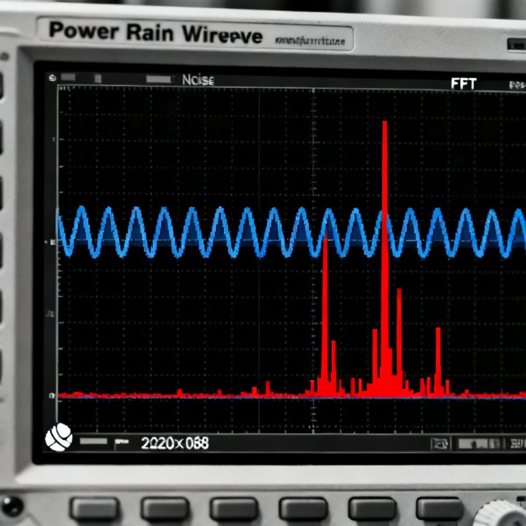
- Impedance Profile: Check TDR (Time Domain Reflectometry) for impedance discontinuities at via transitions and plane crossings.
- Loop Inductance: Calculate the loop inductance of the return path for critical signals. Keep it below 1 nH for signals above 1 GHz.
- EMI Scan: Perform a near-field scan of the BGA area to identify radiation hotspots.
Chapter 6: Case Studies and Real-World Examples
Case Study 1: 0.8mm Pitch BGA with 256 Signals
Challenge: Escaping 256 signals from a 0.8mm pitch BGA on a 6-layer board. The designer used dog-bone fanout with through-hole vias. Initial simulations showed severe signal degradation on the top-speed DDR4 interface.
Solution: Added a grid of ground vias in the BGA area (one GND via per 3 signal vias). Moved the DDR4 signals to the inner layers with continuous ground references. Back-drilled all DDR4 vias.
Result: Signal integrity improved by 40% (reduced jitter and eye opening). EMI levels dropped by 6 dB.
Case Study 2: 0.4mm Pitch BGA with HDI
Challenge: A 0.4mm pitch BGA for a mobile processor required 400+ signals. Standard through-hole vias were impossible.
Solution: Used stacked microvias (1-2-3-4-3-2-1 HDI stack-up). Ground microvias were placed under the BGA balls for every signal via. All high-speed signals used blind vias to eliminate stubs.
Result: The design achieved 10 Gbps per lane on the PCIe Gen 3 interface with a 0.5 UI eye opening.
Frequently Asked Questions (FAQ)
What is a return path in high-speed PCB design?
The return path is the path that high-frequency return current takes back to the source, flowing directly under the signal trace on the adjacent reference plane. Maintaining a continuous return path is critical for signal integrity.
Why is the return path so important for BGA escape routing?
In BGA escape routing, signals often change layers, which can interrupt the return path if ground vias are not properly placed. A broken return path increases loop inductance and degrades signal quality.
What is the best way to maintain a return path in dense routing areas?
Use continuous reference planes, via stitching, stitching capacitors for plane crossings, and via fences for isolation. Ensure ground vias are placed near every signal via transition.
How does HDI technology help with return path management?
HDI technology allows placing ground microvias directly under BGA balls, providing an extremely short return path. This is essential for ultra-fine pitch BGAs and high-speed interfaces like DDR5.
What are the consequences of a poor return path?
A poor return path leads to increased loop inductance, EMI radiation, crosstalk, and signal degradation. It can cause system failures in high-speed designs.
Meta Description: Master return path PCB design for BGA escape and dense routing areas. Expert guide on signal integrity, via stitching, and HDI techniques for high-speed PCBs.
URL: /return-path-pcb-design-bga-escape