Master the critical concept of return path PCB design for differential pairs to manage common mode return current effectively. This guide covers signal integrity, layout techniques, and practical rules for high-speed PCB design.
Physics of Common Mode Return Current in Differential Pairs
Differential vs. Common Mode Current
A differential pair consists of two traces (P and N) carrying equal amplitude but opposite polarity signals. The differential mode current flows from the driver to the receiver on one line and returns on the other line. In an ideal, perfectly balanced system, no net current flows to ground. However, in reality, the signal is a superposition of differential and common mode components. The common mode current is the average of the two signal currents. It is not canceled and flows in the same direction on both traces. This common mode current must return to the source via a path—typically a ground or power plane. If this return path is interrupted or has high impedance, the common mode current will find the path of least impedance, which often results in increased radiation and susceptibility to noise.
Why Common Mode Exists
Common mode voltage can arise from several sources: driver imbalances, imperfections in the driver circuit cause slight differences in rise/fall times or amplitudes; skew, timing differences between the P and N traces convert some differential energy into common mode; external coupling, nearby aggressor signals can induce common mode noise onto the pair; ground bounce, switching noise on the power distribution network can inject common mode current.
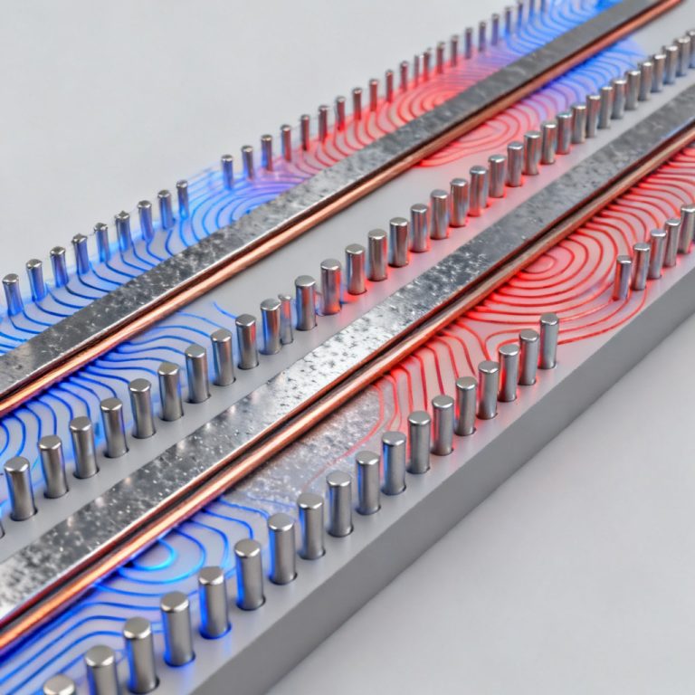
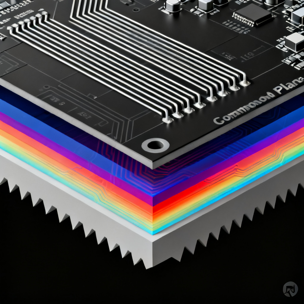
The Return Path is a Ground Plane
The return path for common mode current is not a “virtual ground”—it is a physical structure, typically a solid copper plane. The common mode current flows from the receiver back to the driver through the ground plane. The return current density is concentrated directly under the differential pair, following the path of least inductance. Any discontinuity, such as a split in the plane, a void, or a change in reference layer, forces the return current to detour, increasing loop area and inductance. This leads to increased radiated emissions, higher crosstalk, and degraded signal integrity (increased jitter and noise margin reduction).
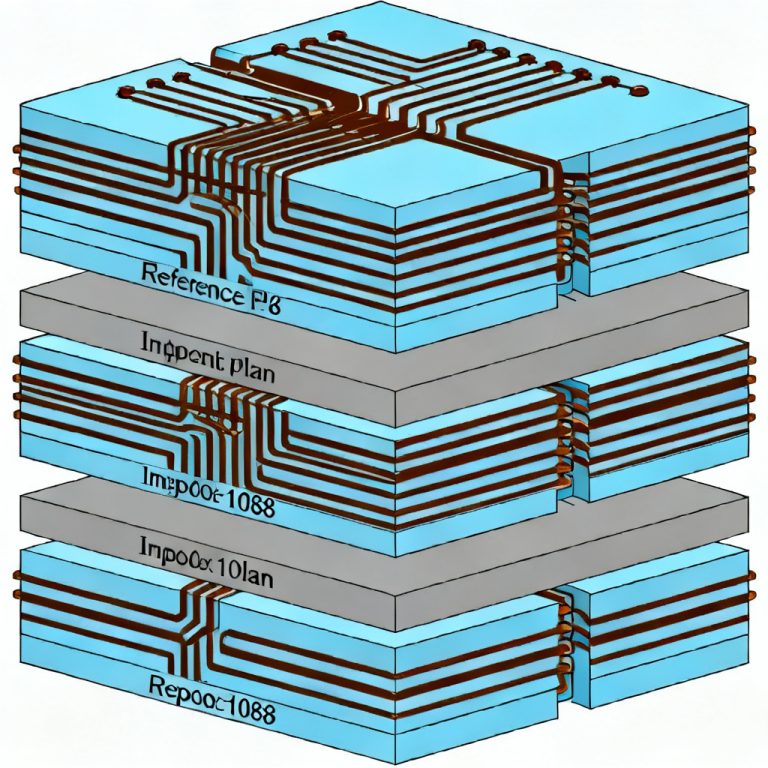
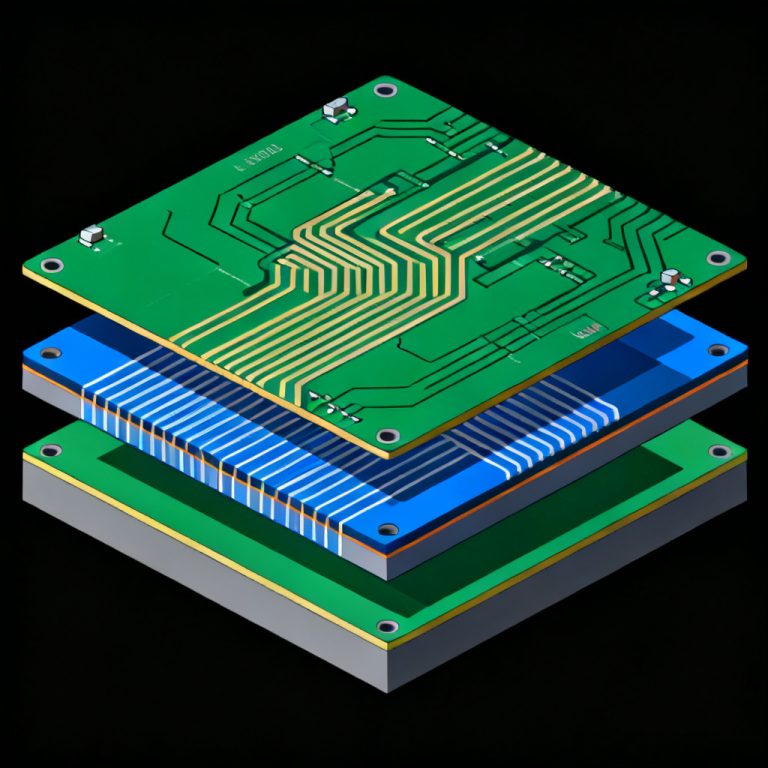
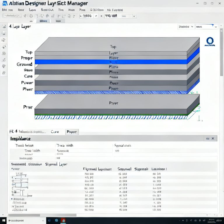
PCB Stackup and Reference Plane Design for Common Mode Return
Solid, Unbroken Reference Planes
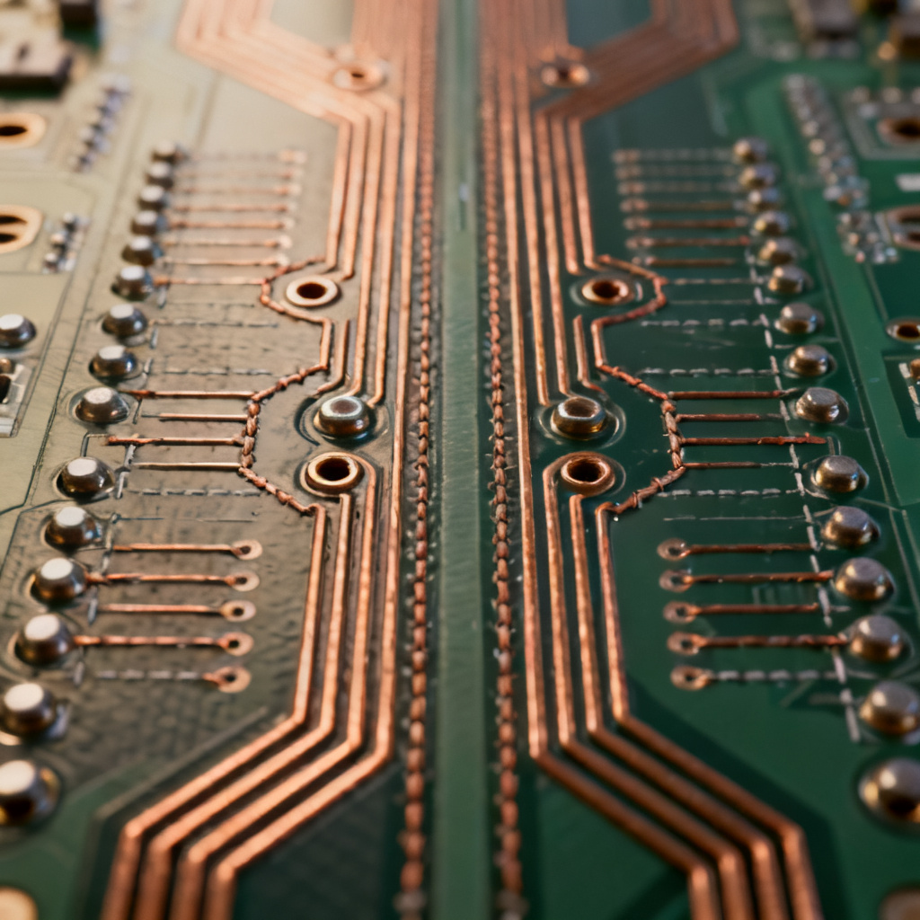
The most critical rule for managing common mode return current is to provide a continuous, unbroken ground plane directly adjacent to the differential pair layer. This plane must be a ground plane, not a power plane, because a ground plane provides a lower impedance and more predictable return path for common mode currents. It must be solid, avoiding splits, slots, or large cutouts under the differential pair. Even a narrow gap can force the return current to take a longer path, increasing loop area. The plane should be close to the signal layer; the distance between the signal layer and the reference plane (the dielectric thickness) determines the impedance of the common mode return path. A thinner dielectric reduces the loop area and inductance.
Stackup Recommendations
For high-speed differential pairs, a standard stackup might be: Top Layer with differential pairs (microstrip), Layer 2 as ground plane (solid), Layer 3 as power plane (or secondary routing), and Bottom Layer as ground plane (or secondary routing). If you must route differential pairs on an inner layer (stripline), ensure the adjacent layers are solid ground planes. For example, in a 6-layer stackup: L1 signals, L2 ground, L3 stripline differential pairs, L4 ground, L5 power, L6 signals.
The Problem with Power Planes as Return Paths
While a power plane can theoretically act as a return path for common mode current (because it is AC-coupled to ground through bypass capacitors), it is not ideal. The impedance of a power plane is higher than a ground plane due to the series inductance of the capacitors. Additionally, the return path is not as directly below the signal as it would be with a ground plane. Therefore, always prefer a ground plane as the immediate reference for differential pairs.
Via Design and Stitching for Return Path Continuity
The Via Discontinuity Problem
When a differential pair changes layers (e.g., from top layer to inner layer), the signal vias create a discontinuity in the return path. The common mode current must also transition from one reference plane to another. If there is no via connecting the two reference planes near the signal vias, the return current will seek an alternative path, often through parasitic capacitance or through a longer loop, causing impedance mismatch and radiation.
The Solution: Ground Stitching Vias
To maintain a low-impedance return path when transitioning layers, place ground stitching vias as close as possible to the differential pair vias. The rule is to place one ground via for every signal via in the differential pair. The ground vias should be located within 30-50 mils (0.75-1.25 mm) of the signal vias. The ground vias should connect the reference planes on both layers. For example, if a differential pair transitions from Layer 1 (reference: Layer 2 ground) to Layer 3 (reference: Layer 4 ground), place a ground via near the signal vias that connects Layer 2 and Layer 4.
Optimizing Stitching Via Placement
Symmetry is key: place ground vias symmetrically around the differential pair to maintain balance. For very high-speed signals (e.g., >10 Gbps), use multiple ground vias (e.g., two or three) to reduce inductance. In extreme cases, consider via-in-pad with ground vias directly adjacent to the signal vias.
Avoiding Return Path Disruption at Connectors
When a differential pair exits a PCB through a connector (e.g., HDMI, USB, Ethernet), the return path continuity is critical. Ensure that the connector has dedicated ground pins that are connected to the ground plane with low inductance. The differential pair vias near the connector should be surrounded by multiple ground vias. The connector’s metal shell should also be tied to the ground plane.
Advanced Routing Techniques for Differential Pairs
Maintaining Impedance Control
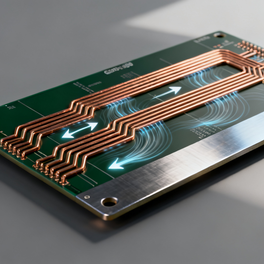
The common mode impedance of a differential pair is just as important as the differential impedance. Common mode impedance is determined by the distance between the traces and the reference plane. To maintain consistent common mode impedance, keep the trace width and spacing constant, maintain a constant distance to the reference plane (i.e., avoid changing layers without proper stitching), and use a consistent dielectric material and thickness.
Avoiding 90-Degree Bends
While 90-degree bends are not as catastrophic as once thought, they can cause impedance discontinuities and increase common mode conversion. Use 45-degree chamfered bends or curved traces for better signal integrity.
Skew Compensation
Skew between the P and N traces converts differential mode energy into common mode. To minimize skew, match the lengths of the two traces to within the tolerance specified by the protocol (e.g., 5 mils for USB 3.0). Use meandering traces to add length to the shorter trace. Ensure the meanders are symmetric and maintain the same spacing between the two traces.
Routing Over Plane Splits
Never route differential pairs over a split in a ground plane. Even if the split is narrow, it forces the common mode return current to detour, increasing loop area and radiation. If you must cross a split (e.g., from an analog to a digital ground), use a bridge or a stitching capacitor to provide a return path.
Guard Traces and Ground Pour
Guard traces (grounded copper traces running alongside the differential pair) are sometimes used to isolate the pair from adjacent signals. However, they can also affect impedance and increase crosstalk if not properly designed. If you use guard traces, keep them at least 3 times the trace width away from the differential pair. Connect them to ground with multiple vias at regular intervals (e.g., every 1/10 of the wavelength at the highest frequency). Ground pour (copper fill) around differential pairs is generally not recommended because it can create impedance discontinuities and increase common mode current. If you must use ground pour, keep it at least 5 times the dielectric thickness away from the traces.
Simulation and Validation of Return Path Design
Using 3D EM Solvers
To verify the return path design, use 3D electromagnetic (EM) simulation tools. These can show the current density distribution in the ground plane and identify areas where the return path is disrupted. Key parameters to check include common mode impedance, which should be consistent along the entire trace; return current density, which should be concentrated under the traces, not detouring around voids; and radiated emissions, to simulate the far-field radiation to ensure compliance with EMI standards.
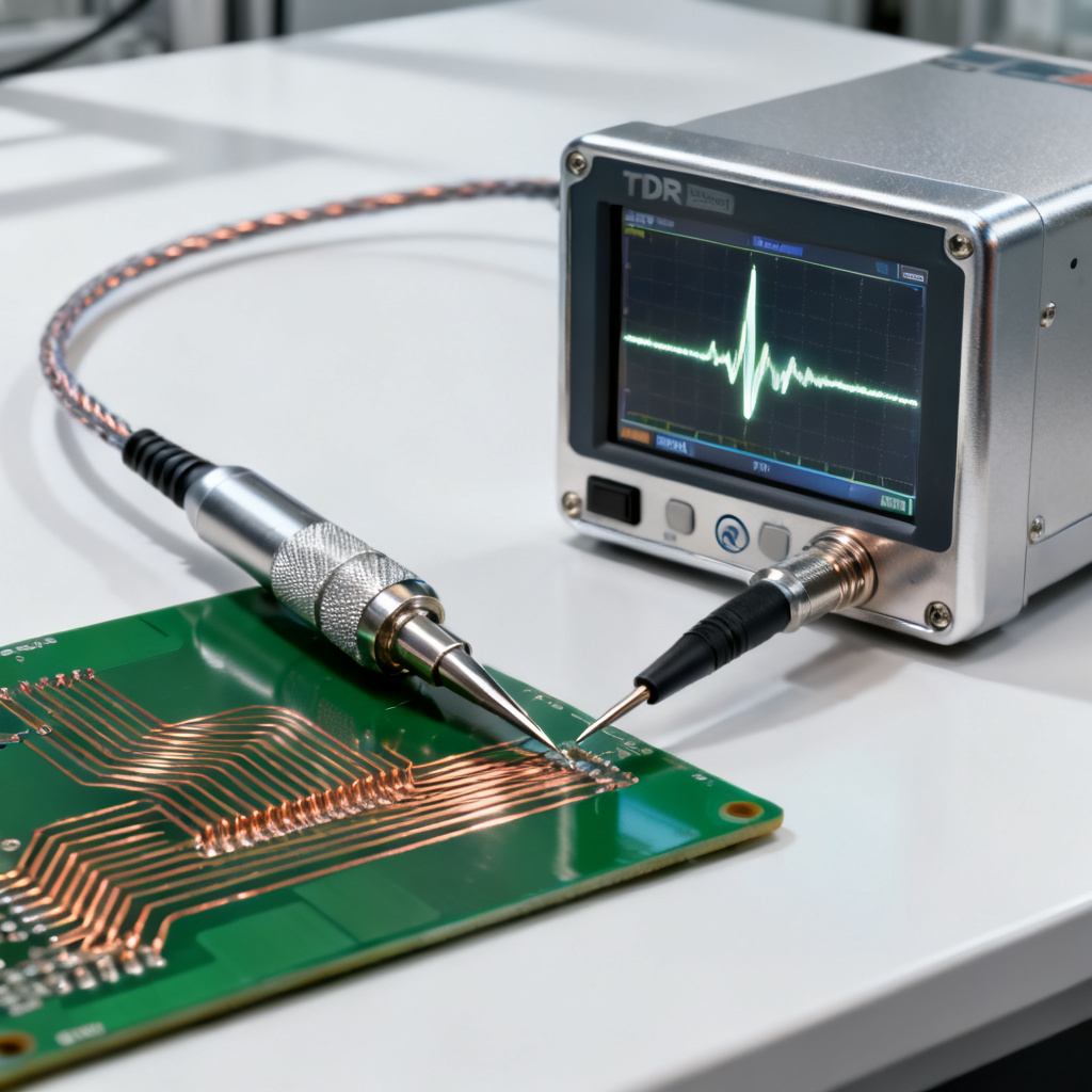
Time-Domain Reflectometry (TDR) Verification
On a physical prototype, use TDR measurements to check for impedance discontinuities. A sudden impedance change at a via or a plane split indicates a return path problem.
Common Mode Filtering
If common mode noise is unavoidable (e.g., due to connector or cable effects), add common mode chokes or ferrite beads at the driver or receiver. However, this should be a last resort—proper layout design is always preferable.
Common Mistakes and How to Avoid Them
| Mistake | Consequence | Solution |
|---|---|---|
| Routing over a ground plane split | Increased EMI, signal integrity degradation | Use a solid reference plane; if split is unavoidable, use a bridge or stitching capacitor. |
| Neglecting ground vias at layer transitions | Return path discontinuity, impedance mismatch | Place ground vias near signal vias. |
| Using a power plane as the primary reference | Higher impedance, unpredictable return path | Use a ground plane directly adjacent to the signal layer. |
| Ignoring skew | Increased common mode conversion | Match trace lengths precisely. |
| Over-reliance on guard traces | Impedance variation, increased crosstalk | Keep guard traces far away or avoid them entirely. |
| Placing vias too far from the connector | High inductance at the connector interface | Place multiple ground vias near connector ground pins. |
Industry Terminology for Common Mode Return Current
Common mode return current refers to the portion of current that flows in the same direction on both traces of a differential pair, requiring a low-impedance path through a reference plane. Signal integrity is the measure of signal quality in high-speed PCB design, directly impacted by return path continuity. Impedance control ensures consistent characteristic impedance along traces, crucial for minimizing reflections. Differential pair routing involves two coupled traces designed for noise immunity. EMI (Electromagnetic Interference) is unwanted radiation caused by improper return path design. Via stitching uses multiple vias to connect ground planes, reducing inductance at layer transitions. Skew is the timing mismatch between P and N traces, which increases common mode noise. Return path discontinuity occurs when the reference plane is interrupted, leading to signal degradation.
FAQ
What is the return path for common mode current in differential pairs?
The return path for common mode current in differential pairs is a solid ground plane directly adjacent to the signal layer. This ensures low impedance and minimizes EMI in high-speed PCB design.
Why is ground stitching important for return path PCB design for differential pairs?
Ground stitching is critical for return path PCB design for differential pairs because it maintains continuity when signals change layers, preventing impedance discontinuities and reducing common mode noise.
How does skew affect common mode return current?
Skew converts differential energy into common mode current, which then requires a clean return path. Managing skew is essential for return path PCB design for differential pairs to maintain signal integrity.
Can a power plane serve as a return path for differential pairs?
While possible, a power plane is not ideal for return path PCB design for differential pairs due to higher impedance. A dedicated ground plane is preferred for reliable common mode return current management.
What are the consequences of routing over plane splits?
Routing over plane splits disrupts the return path, increasing loop area, EMI, and signal degradation. This is a common mistake in return path PCB design for differential pairs that must be avoided.