Target impedance curve power integrity PCB design overview showing PDN simulation
To generate a target impedance curve for your power integrity PCB design, you must first understand how the power distribution network (PDN) delivers stable voltage to high-speed devices. This curve defines the maximum allowable PDN impedance across frequency, directly impacting signal integrity and overall performance.
Step 1: Define Core Parameters for Target Impedance Curve
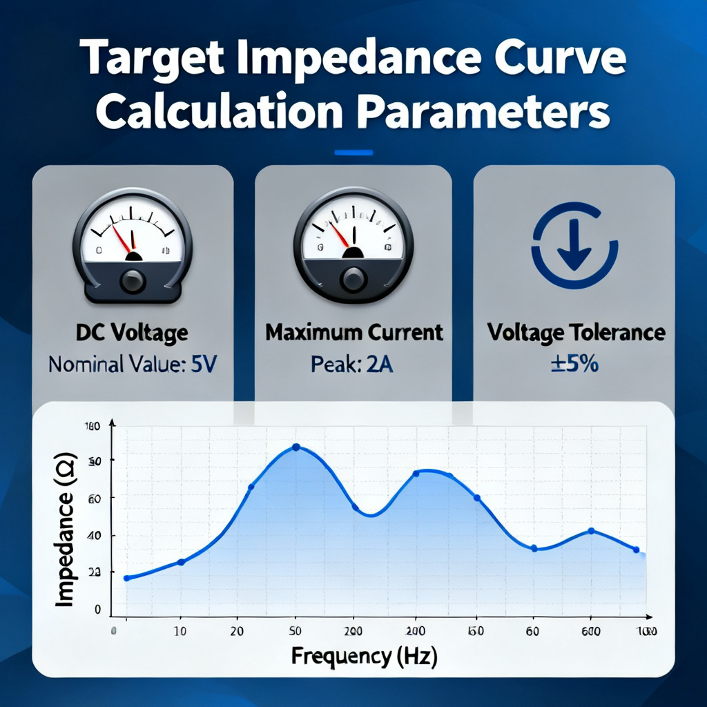
The target impedance curve calculation begins with key device parameters: DC voltage (Vdd), maximum current (Imax), and voltage tolerance (ΔV). For example, a 1.0V rail with ±3% tolerance and 10A current yields Ztarget = 0.03V / 10A = 3 mΩ. This value sets the baseline for your entire power integrity PCB design.
Voltage Tolerance and Transient Current
Voltage tolerance (ΔV) and transient current (ΔI) are the two critical inputs. The formula Ztarget = ΔV / ΔI assumes worst-case transient conditions. In high-speed PCB design, always use the maximum current step to ensure robust PDN performance.
Multi-Rail Considerations
When multiple power rails share a common PDN, calculate Ztarget for each rail separately. The most stringent rail dictates the overall impedance requirement. This ensures all active devices receive clean power.
Step 2: Determine Frequency Range for Target Impedance Curve
The target impedance curve must span from DC to the maximum frequency (Fmax) of the fastest transient event. Use Fmax = 0.35 / Tr, where Tr is the rise time. For a 1 ns rise time, Fmax = 350 MHz. This covers low-frequency VRM behavior, mid-frequency decoupling, and high-frequency plane capacitance.
Low, Mid, and High Frequency Domains
Low frequency (DC to ~10 kHz) is dominated by the voltage regulator module (VRM). Mid frequency (10 kHz to ~10 MHz) relies on bulk and ceramic capacitors. High frequency (10 MHz to Fmax) requires optimized PCB plane capacitance and on-die capacitance.
Step 3: Create the Initial Target Impedance Curve
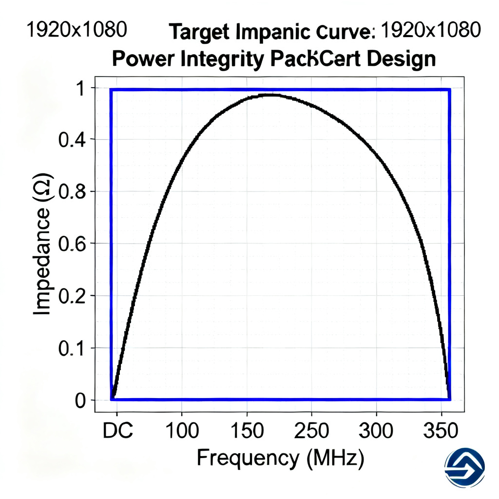
Plot a flat line at Ztarget from DC to Fmax on a log-log scale. This represents the ideal PDN impedance. In real designs, resonances cause peaks, so the goal is to keep the simulated impedance below this line. Use simulation tools like SPICE or Ansys SIwave to validate.
Graphical Representation
The X-axis is frequency (log scale, e.g., 10 Hz to 1 GHz), and the Y-axis is impedance (log scale, e.g., 0.1 mΩ to 100 mΩ). The horizontal line at Ztarget serves as the design constraint.
Step 4: Account for Real-World Limitations
Real-world designs require frequency-dependent Ztarget considerations. At low frequencies, strict impedance is needed; at high frequencies, requirements can relax due to on-die capacitance. Use transient current profiles from simulation for more accurate curves.
Transient Current Profile Analysis
Instead of a single ΔI, use a detailed time-domain current waveform. Convert this to a frequency-domain impedance requirement via Fourier analysis. This yields a more precise target impedance curve for high-speed PCB design.
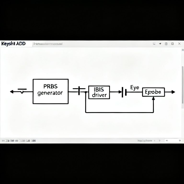
Step 5: Validate with PDN Simulation
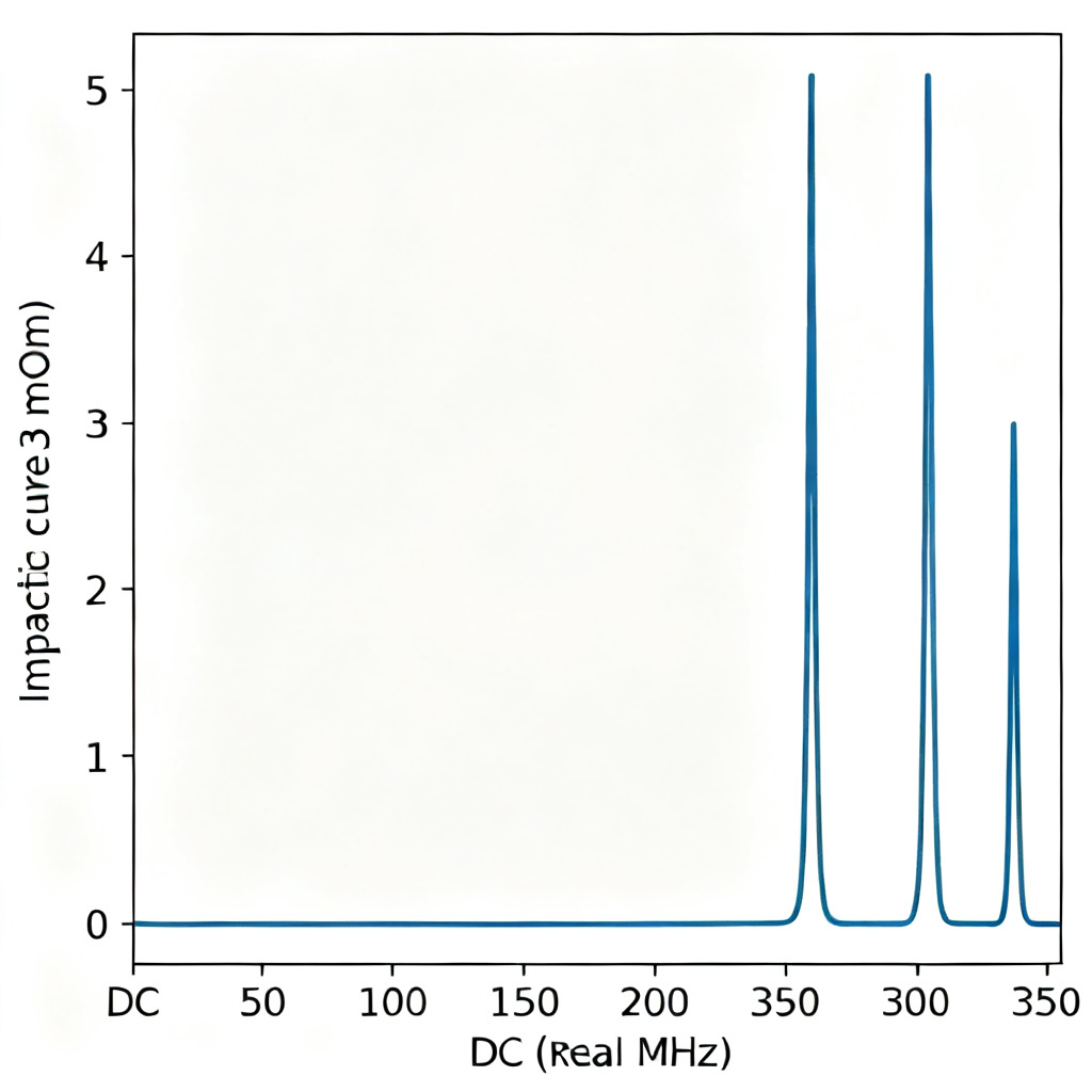
Simulate the actual PDN impedance using tools like Cadence Sigrity or HyperLynx PI. Model the VRM, decoupling capacitors (including ESL and ESR), PCB plane pair, and package inductance. Compare the simulated curve to the target impedance curve.
Interpreting Simulation Results
If the simulated curve exceeds Ztarget at any frequency, add or adjust decoupling capacitors, reduce plane inductance, or modify the stackup. Use a spread of capacitor values to mitigate anti-resonance peaks.
Step 6: Optimize the PDN to Meet the Curve
For low-frequency violations (DC to ~1 MHz), add bulk capacitors (10 µF to 100 µF). For mid-frequency violations (1 MHz to 10 MHz), use ceramic capacitors (0.1 µF to 10 µF) with low ESL. For high-frequency violations (10 MHz to Fmax), increase plane capacitance with thinner dielectrics.
High-Frequency Optimization Techniques
Use multiple vias in parallel to reduce via inductance. Add high-frequency decoupling capacitors (100 pF to 1 nF NP0). Place capacitors close to the load to minimize loop inductance.
Step 7: Document and Iterate
Document the target impedance curve with calculated Ztarget, frequency range, and assumptions. Perform corner analysis for temperature, voltage, and process variations. Iterate if layout or device changes occur.
Best Practices for Documentation
Include the formula used, voltage tolerance, transient current assumptions, and a graph showing both target and simulated curves. This ensures traceability and repeatability in power integrity PCB design.
Common Mistakes to Avoid
Avoid using too simple a formula; real devices have complex current profiles. Include package effects—package inductance and on-die capacitance significantly affect high-frequency impedance. Do not assume a flat curve above Fmax; keep impedance low to prevent noise coupling.
Temperature and DC Bias Effects
Capacitor values (especially X5R/X7R) drop with temperature and DC bias. Always use de-rated values in simulation to ensure accurate target impedance curve compliance.
Target Impedance Curve Parameter Table
| Parameter | Symbol | Example Value | Impact on Target Impedance Curve |
|---|---|---|---|
| DC Voltage | Vdd | 1.0 V | Sets baseline for voltage tolerance |
| Maximum Current | Imax | 10 A | Determines transient current ΔI |
| Voltage Tolerance | ΔV | 30 mV (3%) | Directly used in Ztarget formula |
| Transient Current | ΔI | 10 A | Worst-case for Ztarget calculation |
| Target Impedance | Ztarget | 3 mΩ | Design constraint for PDN |
| Maximum Frequency | Fmax | 350 MHz | Defines frequency range of curve |
Frequently Asked Questions
What is a target impedance curve in power integrity PCB design?
The target impedance curve defines the maximum allowable impedance of the power distribution network across frequency. It ensures stable voltage delivery to high-speed devices, directly impacting signal integrity.
How do I calculate the target impedance curve for my PCB?
Use the formula Ztarget = ΔV / ΔI, where ΔV is voltage tolerance and ΔI is transient current. For example, a 1.0V rail with 3% tolerance and 10A current yields Ztarget = 3 mΩ. This sets the baseline for your power integrity PCB design.
What frequency range should the target impedance curve cover?
The curve should cover from DC to Fmax, where Fmax = 0.35 / Tr (rise time). For a 1 ns rise time, Fmax = 350 MHz. This includes low-frequency VRM, mid-frequency decoupling, and high-frequency plane capacitance effects.
How do I optimize my PDN to meet the target impedance curve?
Add bulk capacitors for low-frequency violations, ceramic capacitors for mid-frequency, and increase plane capacitance for high-frequency. Use multiple vias to reduce inductance and place capacitors close to the load.
What are common mistakes when generating a target impedance curve?
Common mistakes include using too simple a formula, ignoring package effects, assuming a flat curve above Fmax, and overlooking temperature and DC bias effects on capacitors. Always use de-rated values in simulation.
Our High-Speed PCB Manufacturing vs. Standard Fabrication
Our advanced stackup options with thin dielectrics (2 mil or 4 mil prepreg) enable precise target impedance curve compliance. We offer controlled impedance tolerances down to ±5%, ensuring your PDN meets the most stringent requirements. Unlike standard fabricators, we provide detailed impedance reports and test coupons for validation.
Industry Terminology
PDN (Power Distribution Network): The network that delivers power from the VRM to active devices. ESL (Equivalent Series Inductance): Capacitor parasitic inductance affecting high-frequency performance. Anti-resonance: A high-impedance peak caused by capacitor and plane inductance interaction. On-die capacitance: Capacitance within the chip that filters high-frequency noise.