In high-speed PCB design, mastering how to use current density plots to validate return path PCB design is critical for signal integrity and EMI compliance. This guide provides a comprehensive workflow for engineers.

Understanding the Physics: Why Current Density Reveals Return Path Problems
Before diving into plots, understand the physics they visualize. At high frequencies (above 1 MHz), return current follows the path of least inductance, not least resistance, directly under the signal trace on the adjacent reference plane. A current density plot maps this current magnitude, revealing key principles:
- Skin Effect and Proximity Effect: Current concentrates on conductor surfaces and near the signal trace. A valid return path shows a concentrated, narrow high-density band directly beneath the trace.
- Ground Bounce and Simultaneous Switching Noise (SSN): Multiple switching signals share a common impedance path. Plots show “hot spots” where return currents converge, indicating voltage drop areas.
- Loop Area: Enclosed by signal and return paths. Larger loops equal higher inductance and EMI. Plots visualize loops: forced detours show meandering, low-density paths.
Key takeaway: A valid design shows a high-density, narrow, continuous current stripe directly under the signal trace on the reference plane. Any deviation indicates a problem.
Three Critical Scenarios Where Current Density Plots Are Indispensable
Based on comprehensive industry guidance, three primary scenarios make these plots your most powerful validation tool.
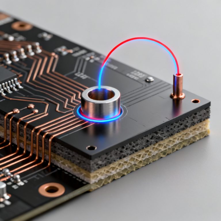
Scenario A: Validating Return Path Across Ground Plane Splits and Moats
The Problem: Ground plane splits (e.g., for analog/digital isolation) disrupt return paths. When a high-speed trace crosses a split, return current must find a longer alternative path around it.

How to Use the Plot:
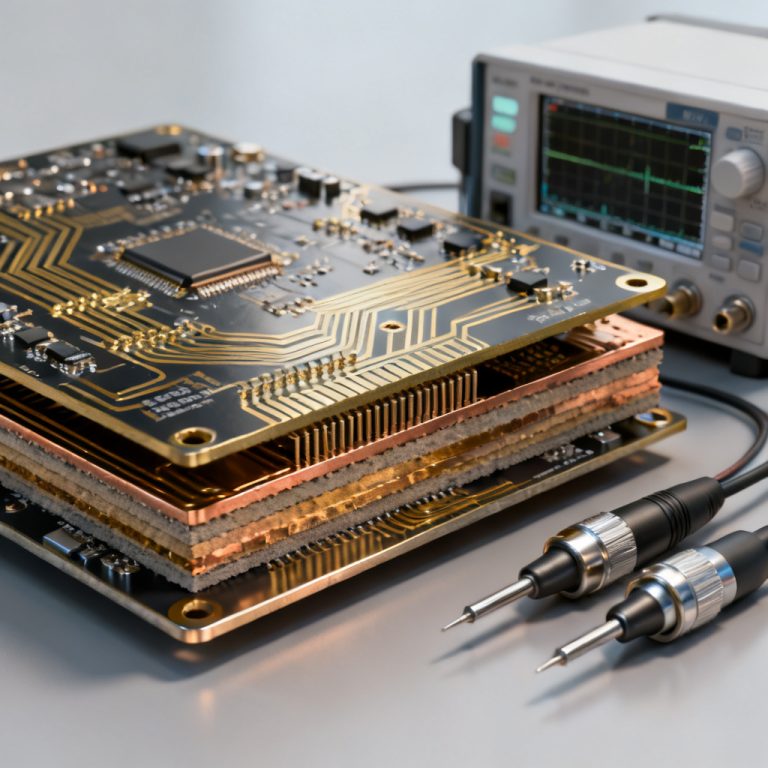
- Setup: Run a 3D EM simulation (e.g., Ansys HFSS, CST) of your PCB stack-up. Place ports at driver and receiver of the critical trace. Request a current density plot on the reference plane at the operating frequency.
- What to Look For: A sharp discontinuity in the high-density current stripe at the split location. You will see a wide, low-density path detouring around the split’s edge.
- Validation Metric: A valid design shows a continuous, high-density return path. A drop of >50% in peak current density magnitude indicates a serious impedance discontinuity.
Mitigation (Validated by Plot): Place a stitching capacitor or bridge trace across the split. Re-run simulation. The plot should now show a high-density path through the capacitor.
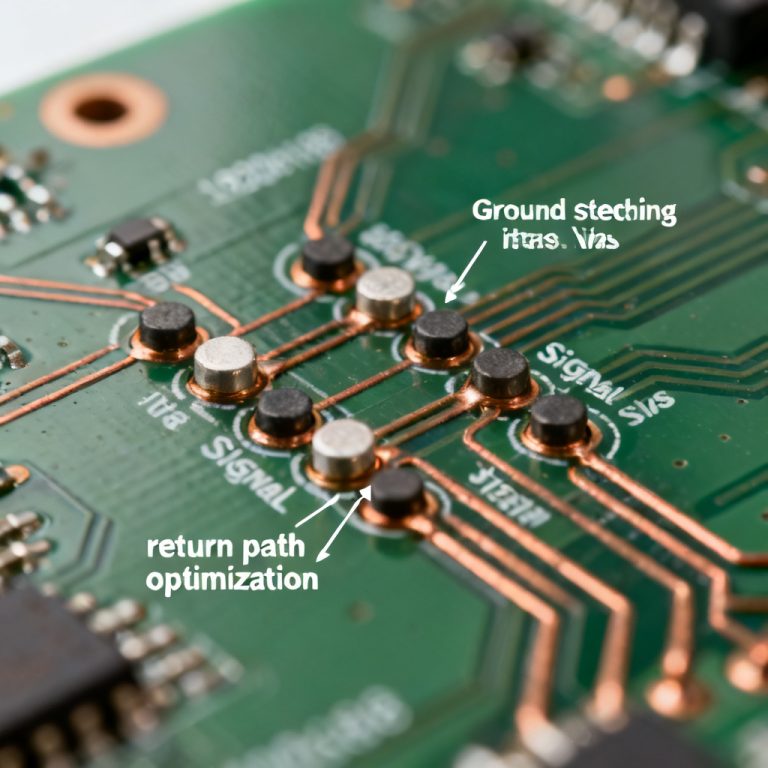
Scenario B: Checking Via Stitching and Ground Via Density
The Problem: When a signal transitions layers, return current must also transition via ground vias near the signal via. Insufficient density or poor placement forces lateral travel, creating large loops.
How to Use the Plot:
- Setup: Focus on a specific signal via transition. Plot 3D current density on all layers involved, especially reference planes.
- What to Look For: A valid design shows a uniform, high-density ring around ground vias stitched to the signal via. Poor stitching shows current spreading across the plane.
- Quantitative Validation: For a single signal via, you need at least 3-4 ground vias within 1/20th of the signal wavelength. If one ground via carries >80% of the current, stitching is unbalanced.
Mitigation (Validated by Plot): Add more ground vias symmetrically around the signal via. Re-run simulation. The plot should show balanced, high-density distribution across all ground vias.
Scenario C: Identifying EMI and Radiated Emission Hotspots
The Problem: Areas where return current takes long, meandering paths act as loop antennas, radiating EMI.
How to Use the Plot:
- Setup: Use a full-wave solver to compute radiated emissions. Correlate emission hotspots with the current density plot.
- What to Look For: “Hot loops” – regions with high current density but not under the signal trace. Found at plane edges, connector areas, and slots.
- Validation Metric: A hotspot with density >3x the average is a strong candidate for EMI trouble.
Mitigation (Validated by Plot): Add a ground fence (row of vias) along the PCB edge near the hotspot, or place a shield can. Re-simulate. Current density at the edge should drop significantly.
Step-by-Step Workflow for Using Current Density Plots
Follow this validated workflow from leading PCB design authorities:
Step 1: Pre-Simulation Setup
- Define Critical Nets: Identify all high-speed clocks, differential pairs, and sensitive analog signals.
- Extract Stack-Up: Export layer stack-up, material properties (Dk, Df, copper roughness), and exact trace geometry from your PCB design tool.
- Set the Frequency: Run simulation at the highest harmonic of the signal (e.g., 5th harmonic for a 1 GHz clock).
Step 2: Run Simulation and Generate Plots
- Choose the Solver: Use a 3D full-wave solver (e.g., Ansys HFSS, CST) for accurate visualization.
- Enable Current Density Visualization: Request a surface current density plot (Jsurf) on all reference planes.
- Set Dynamic Range: Adjust color scale to highlight differences (20 dB dynamic range recommended).
Step 3: Analyze Plots for Three Scenarios
- Check for Continuity: Is there a continuous high-density stripe under each critical trace? (Scenario A)
- Check for Via Density: Are ground vias carrying balanced high-density current? (Scenario B)
- Check for Edge Effects: Is high-density current pushed to PCB edges or around slots? (Scenario C)
Step 4: Iterate and Validate Fixes
- Implement mitigations (stitching vias, capacitors, ground fences).
- Re-run simulation.
- Pass/Fail Criteria: Pass: continuous high-density stripe directly under trace, no hotspots at edges, balanced via current sharing. Fail: broken or meandering stripe, hotspots at edges, one via carries >80% current.

Advanced Techniques and Common Pitfalls
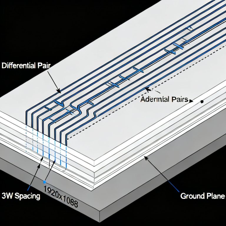
Advanced Technique: Differential Pair Return Path Validation
For differential pairs, use a common-mode current density plot on the reference plane. A valid design shows near-zero current density. Significant density indicates common-mode conversion from asymmetry.
Common Pitfall 1: Ignoring the Power Plane
Both power and ground planes carry return current. For signals referenced to a power plane, plot current density on that plane. Interruptions are as problematic as split ground planes.
Common Pitfall 2: Misinterpreting Color Scales
Always check the legend. A “red” area might be insignificant if the dynamic range is 0-1 A/m. Read numerical values, not just colors.
Common Pitfall 3: Not Simulating at the Right Frequency
A return path good at 100 MHz might fail at 1 GHz. Simulate at the highest frequency component of your signal.
Comparison: Current Density Plots vs. Traditional Rule-of-Thumb Checks
| Validation Method | Current Density Plot | Traditional Rule-of-Thumb |
|---|---|---|
| Return path continuity | Quantitative visualization of current flow | Qualitative visual inspection |
| Via stitching adequacy | Balanced current distribution across vias | Count-based guidelines |
| EMI hotspot detection | Pinpoint high-density areas at edges/slots | General spacing rules |
| Frequency-dependent behavior | Simulates at actual operating frequencies | Static, frequency-agnostic |
Industry Terminology Explained
- Return Path: The path taken by current returning to its source, critical for signal integrity.
- Ground Bounce: Voltage fluctuation on ground plane due to shared return current impedance.
- Stitching Via: A via connecting ground planes to provide a low-inductance return path.
- Loop Area: The area enclosed by signal and return paths, directly proportional to inductance and EMI.
- Full-Wave Solver: A 3D electromagnetic simulation tool that solves Maxwell’s equations for accurate field visualization.
FAQ: Current Density Plots for Return Path Validation
What is a current density plot in PCB design?
A current density plot is a visual representation of how return current distributes across reference planes, helping engineers validate return path integrity in high-speed PCB designs.
How do I use current density plots to validate return path design?
Use them to check for continuous high-density stripes under traces, balanced via stitching, and absence of edge hotspots, following the workflow outlined above.
Why is return path important in high-speed PCB design?
A poor return path increases loop inductance, causing ground bounce, signal integrity degradation, and EMI. Validating it with current density plots ensures robust performance.
What tools generate current density plots?
3D full-wave solvers like Ansys HFSS, CST Microwave Studio, and Keysight ADS provide accurate current density visualization for return path analysis.
Can current density plots detect EMI issues?
Yes, they identify “hot loops” at plane edges, connectors, and slots where high-density current indicates potential radiated emission sources.