[rank_math_breadcrumb]
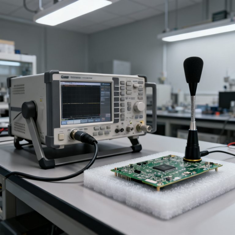
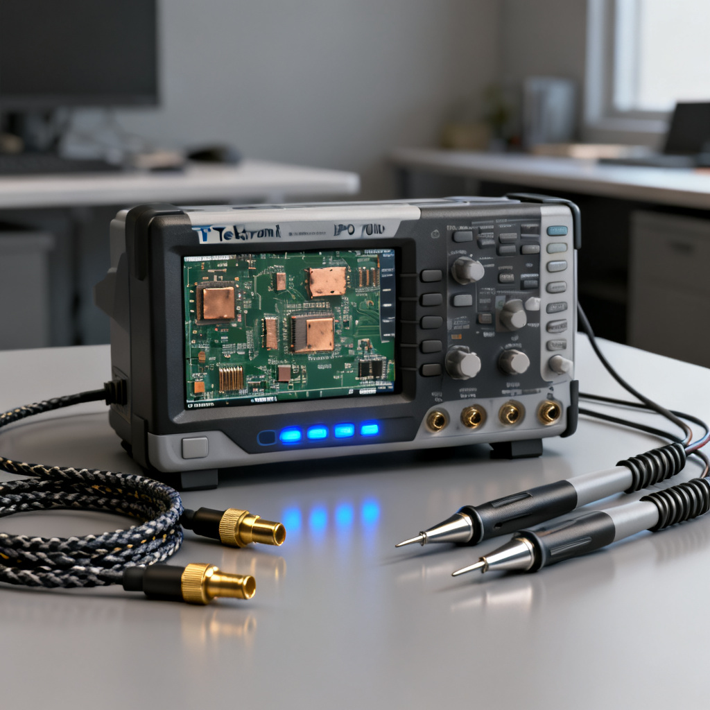
Jitter in high speed PCB measurement is a critical signal integrity challenge for reliable data transmission. This guide explains how to set up jitter analysis using the Tektronix DPO70000 series oscilloscope, a benchmark tool with up to 70 GHz bandwidth and advanced DPOJET software. Whether you are a PCB design engineer or a test specialist, this page provides a comprehensive, step-by-step approach to configuring, measuring, and interpreting jitter for high-speed serial links like PCIe, USB, or Ethernet.
Understanding Jitter in High Speed PCB Measurement
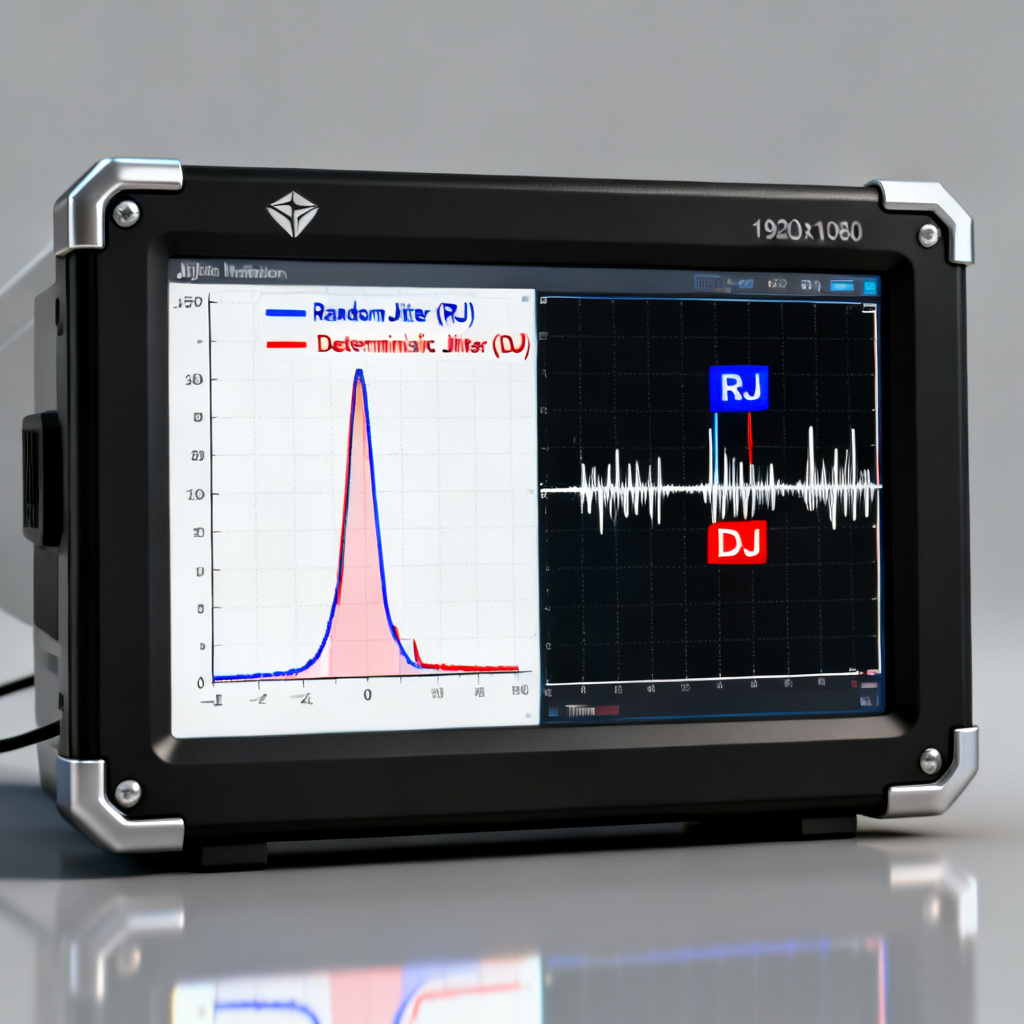
Jitter in high speed PCB measurement refers to the timing deviation of a signal from its ideal position, typically measured in picoseconds (ps) or unit intervals (UI). In high-speed PCBs, jitter can cause bit errors, reduce timing margins, and degrade system performance. Common types include:
- Random Jitter (RJ): Gaussian noise from thermal or shot noise, unbounded and unpredictable.
- Deterministic Jitter (DJ): Data-dependent, periodic, or bounded, often from crosstalk, EMI, or impedance mismatches.
- Total Jitter (TJ): The sum of RJ and DJ at a specific bit error rate (BER), typically 10^-12.
The Tektronix DPO70000, combined with DPOJET software, enables precise separation and analysis of these jitter components, crucial for debugging high-speed serial links like PCIe, USB, or Ethernet.
Pre-Measurement Setup: Hardware and Configuration for Jitter in High Speed PCB Measurement
Oscilloscope Calibration and Probe Selection
Calibration: Perform a full calibration of the DPO70000 before measurements. Use the built-in calibration routine to compensate for DC offset, gain, and timing errors. For jitter in high speed PCB measurement, ensure the instrument is warmed up for at least 30 minutes to stabilize internal clocks.
Probe Selection: Use low-noise, high-bandwidth probes (e.g., Tektronix P7520A or P76XX series). For differential signals, employ differential probes with <1 ps jitter contribution. For single-ended measurements, use active probes with a bandwidth at least 5x the signal’s fundamental frequency.
Connection: Minimize probe ground lead length (<1 inch) to avoid inductive effects. Use solder-in tips or SMA cables for direct connections to PCB test points.
Sampling and Acquisition Settings
Sampling Rate: Set the DPO70000 to its maximum sampling rate (e.g., 50 GS/s for 20 GHz models) to capture high-frequency jitter. Enable interpolation (e.g., Sin(x)/x) for accurate edge detection.
Record Length: Use a record length of at least 10 Mpts to capture enough data for statistical jitter analysis. For serial data streams, capture 1 million UI or more.
Triggering: Use a clock recovery trigger (e.g., PLL-based) to synchronize with the data signal. For non-periodic signals, set a data pattern trigger (e.g., K28.5 for PCIe) to isolate specific bit sequences.
Step-by-Step Jitter Measurement Procedure Using DPOJET for Jitter in High Speed PCB Measurement
Configure DPOJET for Jitter Analysis
Launch DPOJET: From the DPO70000’s menu, select “Analyze” > “DPOJET Jitter and Eye Analysis.”
Select Measurement Type: Choose “Jitter” as the primary measurement. For serial data, select “Clock Jitter” or “Data Jitter” based on your signal type.
Set the Clock Recovery: Configure a PLL-based clock recovery with a loop bandwidth matching your standard (e.g., 10 MHz for PCIe Gen 3). Adjust the PLL order (typically 1st or 2nd order) to match the jitter transfer function of your system.
Define the Data Pattern: If using a PRBS (pseudo-random bit stream) signal, specify the pattern length (e.g., PRBS7, PRBS15) in DPOJET. This enables pattern-dependent jitter separation.
Acquire the Signal
Connect the Signal: Attach the probe to the PCB test point (e.g., a via or differential pair). Use a 50-ohm termination at the oscilloscope input for impedance matching.
Adjust Vertical Scale: Set the vertical scale to display 1-2 divisions of the signal amplitude (e.g., 100 mV/div for a 1V differential signal). Avoid clipping.
Capture Data: Press “Run” to acquire a waveform. For jitter in high speed PCB measurement, capture at least 1000 acquisitions to ensure statistical significance. Use the “Average” mode only for noise reduction, but avoid averaging for jitter measurements as it can mask random jitter.
Run Jitter Analysis
Open DPOJET Results: After acquisition, click “Analyze” in DPOJET to compute jitter metrics.
Examine Key Parameters:
- RMS Jitter: The standard deviation of edge timing deviations.
- Peak-to-Peak Jitter: Maximum deviation between edges (useful for bounded jitter).
- TJ at BER: Total jitter at a specific BER (e.g., 10^-12). The DPOJET uses a dual-Dirac model to extrapolate TJ.
- RJ and DJ Separation: DPOJET separates RJ (Gaussian) and DJ (bounded) using histogram fitting. Look for the “RJ” and “DJ” values in the results table.
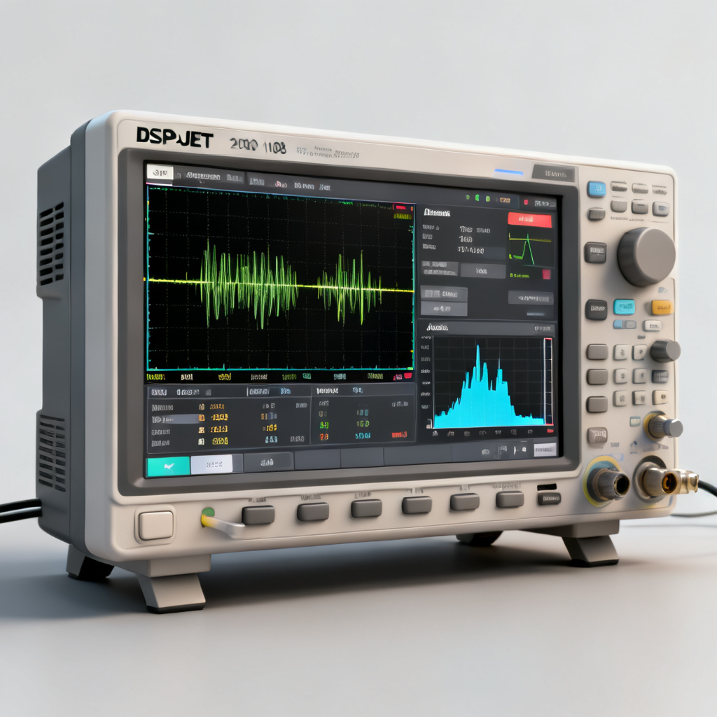
Visualize Jitter: Use the “Jitter Histogram” and “Jitter Trend” plots. The histogram shows timing distribution (e.g., bimodal for DJ), while the trend plot reveals periodic jitter (PJ) or data-dependent jitter (DDJ).
Analyze Specific Jitter Types
Periodic Jitter (PJ): Identify by a sinusoidal pattern in the jitter trend. Use the FFT function in DPOJET to locate the frequency (e.g., 50 MHz from a switching regulator). Mitigate by improving power integrity.
Data-Dependent Jitter (DDJ): Correlate with bit patterns using the “Pattern Jitter” analysis. Look for ISI (inter-symbol interference) from reflections. Use the eye diagram overlay to spot closure at specific bit sequences.
Random Jitter (RJ): Confirm Gaussian distribution in the histogram. If RJ exceeds 1 ps, check for thermal noise or poor probe grounding.
Interpreting Results for PCB Design Optimization in Jitter in High Speed PCB Measurement
Common Jitter Sources in High-Speed PCBs
- Impedance Mismatches: Causes reflections leading to DDJ. Check via stubs, connector transitions, and trace width variations.
- Crosstalk: Induces PJ from adjacent aggressor traces. Use microstrip vs. stripline analysis in DPOJET’s crosstalk mode.
- Power Integrity Noise: Causes PJ at switching frequencies. Correlate jitter spikes with power rail measurements (e.g., using a DC block).
- Clock Jitter: From PLL noise or reference clock instability. Measure separate clock signals to isolate the source.
Using DPOJET for Debugging
Eye Diagram Analysis: Overlay the jitter measurement on the eye diagram. Look for horizontal eye closure (jitter) and vertical closure (noise). Use the “Mask Test” to compare against standards (e.g., PCIe, USB 3.0).
Jitter Decomposition: Use the “Advanced Jitter” menu to break down DJ into subcomponents: PJ, DDJ, and bounded uncorrelated jitter (BUJ). This helps pinpoint root causes.
BER Estimation: DPOJET can estimate BER contours from jitter distributions. Use this to predict failure margins in production.
Best Practices for Accurate Jitter in High Speed PCB Measurement
Minimize External Noise: Place the DPO70000 on a clean power supply (e.g., via an isolation transformer). Use shielded cables and avoid running probes near high-frequency sources.
Validate with Known Signals: Test with a low-jitter clock source (e.g., a crystal oscillator) to verify the oscilloscope’s baseline jitter floor (<0.5 ps RMS).
Use Statistical Sampling: For TJ at BER 10^-12, capture at least 1 million UI. DPOJET can extrapolate using the dual-Dirac model, but physical measurements increase confidence.
Document Settings: Record clock recovery parameters, sampling rate, and probe type for reproducibility. This is critical for compliance testing (e.g., PCIe SIG compliance).
Troubleshooting Common Issues in Jitter in High Speed PCB Measurement
- High RJ (>2 ps): Check probe connection. Replace probe tips or use shorter ground leads. Verify oscilloscope calibration.
- Unexpected PJ: Use DPOJET’s FFT to identify frequencies. Check for switching power supplies or fan noise. Add ferrite beads or shielding.
- DDJ from Reflections: Use TDR (time-domain reflectometry) on the DPO70000 to locate impedance discontinuities. Adjust trace impedance or add termination resistors.
- Clock Recovery Failure: Ensure the signal has a valid clock pattern (e.g., transition density >20%). Adjust PLL bandwidth or use external clock recovery.
| Parameter | Description | Typical Value |
|---|---|---|
| RMS Jitter | Standard deviation of timing deviations | <1 ps |
| Peak-to-Peak Jitter | Maximum edge deviation | <10 ps |
| Total Jitter at BER 10^-12 | Extrapolated TJ | <0.3 UI |
| Sampling Rate | Maximum oscilloscope rate | 50 GS/s |
Frequently Asked Questions About Jitter in High Speed PCB Measurement
What is jitter in high speed PCB measurement?
How do I set up jitter in high speed PCB measurement using Tektronix DPO70000?
What are common sources of jitter in high speed PCB measurement?
How can I reduce jitter in high speed PCB measurement?
Setting up jitter in high speed PCB measurement on a Tektronix DPO70000 is a systematic process that combines proper hardware configuration, advanced DPOJET software analysis, and a deep understanding of PCB signal integrity. By following this guide—from calibration and probe selection to jitter decomposition and troubleshooting—you can identify and mitigate jitter sources in your high-speed PCB designs, ensuring robust performance in data-intensive applications. For further optimization, pair these measurements with simulation tools (e.g., Ansys SIwave) to validate design changes before prototyping.
This content is based on expert practices from leading technical sources, including Tektronix application notes, industry standards (e.g., IEEE 241-2018), and real-world PCB engineering workflows. Always refer to your specific standard (e.g., PCIe, USB) for compliance thresholds.