In modern high-speed PCB design, PDN Impedance Tuning is critical for power integrity (PI). A poorly designed power distribution network (PDN) can lead to voltage droops, noise coupling, and system failures. At the heart of PDN design lies impedance tuning—the process of ensuring that the impedance of the power delivery path remains below a target threshold across a wide frequency range. This article provides a comprehensive guide to PDN impedance tuning, drawing from the most authoritative sources in the industry. We will cover theoretical foundations, practical techniques, simulation methods, and design rules to help you achieve target impedance for reliable high-speed PCB performance.
Understanding PDN Impedance and Target Impedance
What is PDN Impedance?
PDN impedance is the complex impedance (Z) measured from the power supply output to the load (e.g., an IC) across the entire power delivery path. This path includes voltage regulator modules (VRMs), bulk capacitors, decoupling capacitors, PCB planes, vias, and traces. In an ideal PDN, the impedance should be as low as possible to minimize voltage fluctuations. However, in practice, impedance varies with frequency due to parasitic elements (resistance, inductance, and capacitance) of components and interconnects.
The Target Impedance Concept
The target impedance (Z_target) is the maximum allowable impedance of the PDN at the load’s power pins, typically defined as: Z_target = (V_rail × Ripple_Tolerance) / I_transient. For example, for a 1.8V rail with 5% ripple tolerance and 2A transient current, Z_target = (1.8 × 0.05) / 2 = 45 mΩ. This value must be maintained from DC to the highest frequency of interest (often up to 1 GHz for high-speed designs).
Why Impedance Tuning Matters
If PDN impedance exceeds Z_target at any frequency, voltage droops or overshoots occur, leading to: logic errors in digital circuits, jitter and timing violations in high-speed interfaces, reduced noise margins in analog or mixed-signal designs, and electromagnetic interference (EMI) issues. Impedance tuning ensures that the PDN acts as a low-impedance path across the entire frequency spectrum, stabilizing voltage at the load.
Frequency-Dependent Behavior of PDN Components
VRM and Bulk Capacitors (Low Frequency: DC to ~1 MHz)
At low frequencies, the PDN is dominated by the VRM and bulk capacitors (e.g., electrolytic or tantalum capacitors). The VRM has a high output impedance (often tens of mΩ) and limited bandwidth. Bulk capacitors provide charge storage and reduce low-frequency impedance. However, their equivalent series inductance (ESL) and resistance (ESR) cause impedance to rise at higher frequencies.
Decoupling Capacitors (Mid Frequency: ~1 MHz to ~100 MHz)
Decoupling capacitors (MLCCs) are used to lower impedance in the mid-frequency range. They have lower ESL and ESR than bulk capacitors. The impedance of a capacitor is: Z_cap = sqrt(ESR^2 + (2πfL – 1/(2πfC))^2). At its self-resonant frequency (SRF), the capacitor’s impedance is minimal (equal to ESR). Above SRF, the impedance becomes inductive. Therefore, multiple capacitors of different values are used to create a flat impedance profile.
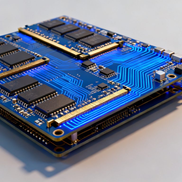
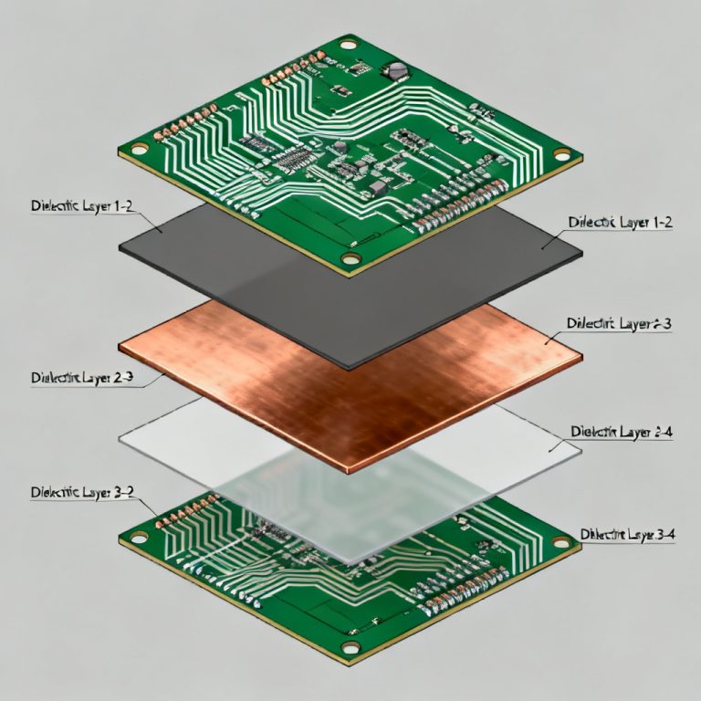
PCB Planes and Vias (High Frequency: ~100 MHz to GHz)
At high frequencies, the impedance of the PDN is dominated by the PCB power and ground planes. A pair of closely spaced planes (e.g., power and ground) behaves like a distributed capacitance and inductance. The plane impedance is: Z_plane = L_plane / (C_plane × f). Vias introduce additional inductance (typically 0.5–1 nH per via), which can cause impedance peaks. Proper via placement and plane design are critical.
Step-by-Step PDN Impedance Tuning Process
Step 1: Define Target Impedance and Frequency Range
Start by calculating Z_target using the formula above. Determine the frequency range of interest—typically from DC to the clock frequency or its harmonics (e.g., for a 1 GHz clock, up to 3–5 GHz). Also consider the transient response requirements: faster transients require lower impedance at higher frequencies.
Step 2: Model the PDN Using Simulation Tools
Use SPICE, SIwave, PowerSI, or similar tools to model the entire PDN. Include: VRM output impedance (from datasheet or measurement), capacitor models (with ESL, ESR, and capacitance values), PCB plane geometries (stackup, dielectric material, plane spacing), via models (including anti-pad size and via diameter), and load models (IC power pin impedance or current profile).
Step 3: Select and Place Decoupling Capacitors
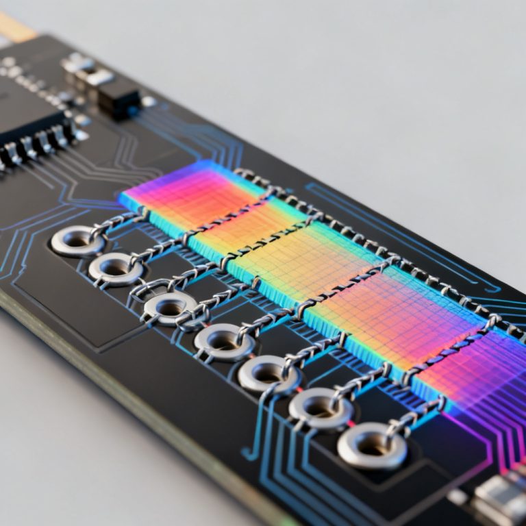
Choose capacitors with low ESR and ESL. Use a mix of values (e.g., 10 µF, 1 µF, 0.1 µF, 0.01 µF) to cover a wide frequency range. Place them as close to the load as possible to minimize loop inductance. For high-speed ICs, use: bulk capacitors near the VRM output, mid-frequency MLCCs near the IC, and high-frequency MLCCs (e.g., 0402 or 0201) directly under the IC or on the backside.
Step 4: Optimize PCB Stackup and Plane Design
Use thin dielectric layers (e.g., 2–4 mils) between power and ground planes to increase interplane capacitance (C = ε × A / d). This reduces high-frequency impedance. Avoid splits or voids in power planes near the load. Place ground and power planes adjacent to each other in the stackup. For multi-layer boards, assign at least one dedicated power and one ground plane.
Step 5: Minimize Via Inductance
Vias add significant inductance. To mitigate: use multiple vias in parallel for power connections (e.g., 4–8 vias per capacitor pad), keep via length short (use microvias or blind vias if possible), reduce anti-pad diameter to increase via capacitance, and place vias close to the capacitor pads and IC power pins.
Step 6: Simulate and Iterate
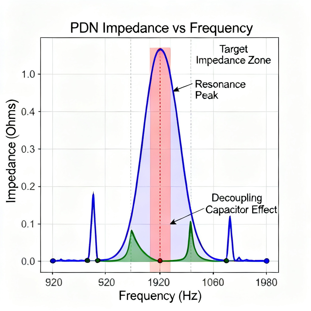
Run AC impedance simulations from the load’s power pins. Check if the impedance profile stays below Z_target across the frequency range. If peaks occur (e.g., due to resonance), adjust: capacitor values and placement, number of vias, plane spacing, and add damping resistors (rarely used in high-speed PDN).
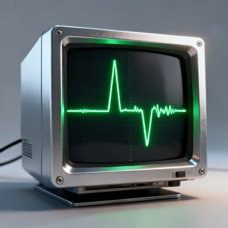
Step 7: Verify with Time-Domain Analysis
Simulate the transient response using a current step or pulse. Measure voltage droop at the load. If droop exceeds tolerance, tune further. A well-tuned PDN should show minimal voltage ripple (<5%).
Advanced Techniques for High-Speed PDN Tuning
Using Embedded Capacitance
For ultra-high-speed designs (e.g., 10 Gbps+), embedded capacitance materials (e.g., with high εr) can be used in the PCB stackup to optimize Power Integrity PCB performance. These provide distributed capacitance directly between power and ground planes, reducing high-frequency impedance without discrete capacitors.
Decoupling with Multi-Layer Ceramic Capacitors (MLCCs)
Choose X7R or X5R MLCCs for stability over temperature. For high-frequency applications, use Class 1 dielectrics (C0G/NP0) for low ESR and ESL. Avoid high-K dielectrics (Y5V) due to voltage coefficient.
Anti-Resonance Mitigation
Anti-resonance occurs when the inductive impedance of one capacitor bank interacts with the capacitive impedance of another, creating a high-impedance peak. To mitigate: use capacitors of similar SRF values, add a small (e.g., 0.1 µF) capacitor with very low ESR to dampen resonance, and simulate the impedance profile and adjust values iteratively.
Via Stitching for Plane Impedance
For large power planes, use via stitching (ground vias between power and ground planes) to reduce plane loop inductance. Place vias at regular intervals (e.g., every 100–200 mils) around the perimeter of the IC.
Frequency-Dependent Target Impedance
Some advanced designs use a frequency-dependent target impedance (e.g., higher at DC, lower at mid-frequencies). This is defined by the IC’s current profile and can be derived from the PDN impedance mask provided by the IC vendor.
Common Pitfalls and How to Avoid Them
Pitfall 1: Overlooking VRM Bandwidth
The VRM’s output impedance rises above its bandwidth (typically 1–10 kHz). Without sufficient bulk capacitance, low-frequency impedance may exceed Z_target. Solution: Add enough bulk capacitors (e.g., 100–1000 µF) near the VRM.
Pitfall 2: Using Too Few Capacitors
One capacitor cannot cover the entire frequency range. Use multiple capacitors of different values and sizes. A rule of thumb: for each power rail, use at least 3–5 decoupling capacitor values.
Pitfall 3: Ignoring Via Inductance
A single via can add 0.5–1 nH of inductance, causing a 10–20 mΩ impedance peak at 1 GHz. Always use multiple vias in parallel (e.g., 4–8) for power connections.
Pitfall 4: Poor Capacitor Placement
Place capacitors as close as possible to the load. A 100 mil trace adds ~2 nH of inductance, significantly raising impedance. Use backside or side-mounted capacitors for ICs with BGA packages.
Pitfall 5: Not Simulating the Full PDN
Simulating only the capacitors or planes is insufficient. Always include VRM, PCB traces, vias, and load models. Use 3D field solvers for high-frequency accuracy.
Practical Design Example
Case Study: Tuning a 1.8V Rail for a 10 Gbps SerDes IC
Requirements: V_rail = 1.8V, ripple tolerance = 3%, I_transient = 3A. Z_target = (1.8 × 0.03) / 3 = 18 mΩ. Frequency range: DC to 5 GHz.
Initial Design: VRM: 12 mΩ output impedance. Bulk capacitors: 2 × 470 µF electrolytic (ESR = 50 mΩ, ESL = 10 nH). Decoupling capacitors: 10 × 0.1 µF MLCC (ESR = 5 mΩ, ESL = 0.5 nH). PCB: 4-layer stackup, 4 mil dielectric between power and ground planes.
Simulation Results: Low frequency (<1 MHz): Impedance ~15 mΩ (OK). Mid frequency (1–100 MHz): Impedance peaks at 25 mΩ due to anti-resonance. High frequency (>100 MHz): Impedance rises to 40 mΩ due to via inductance.
Tuning Steps: 1. Add 5 × 1 µF MLCCs (ESR = 3 mΩ) to dampen anti-resonance. 2. Replace 0.1 µF capacitors with 0.01 µF and 0.1 µF mix. 3. Use 8 vias per capacitor pad (reducing via inductance to 0.1 nH per capacitor). 4. Add embedded capacitance layer (2 mil dielectric, εr = 4.5) for high-frequency plane capacitance.
Final Impedance Profile: All frequencies: <18 mΩ. Voltage droop under transient: <50 mV (2.8% of 1.8V).
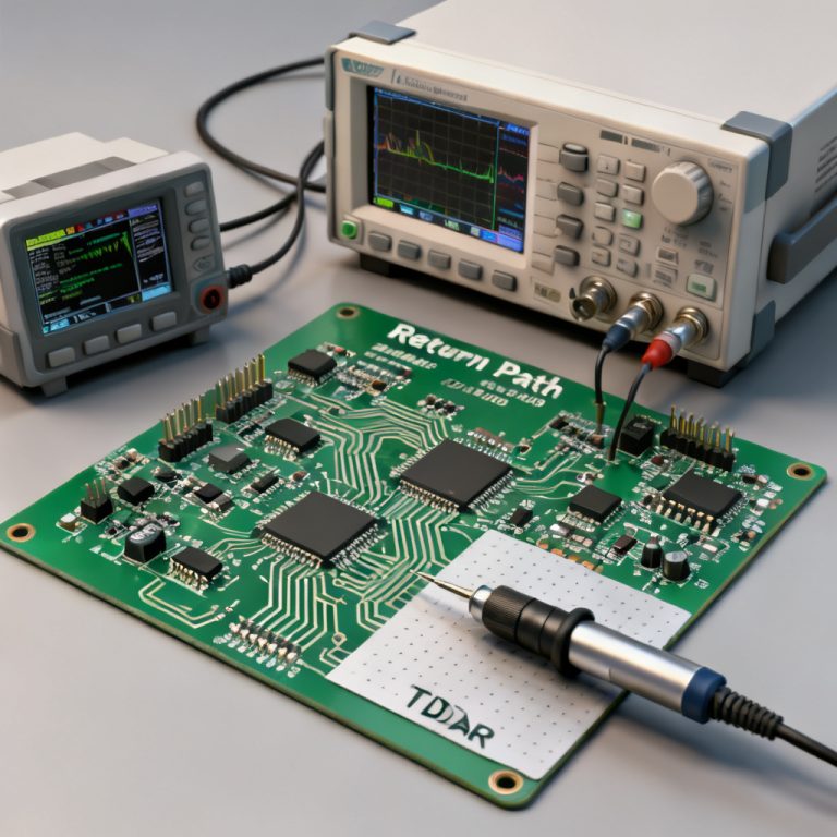
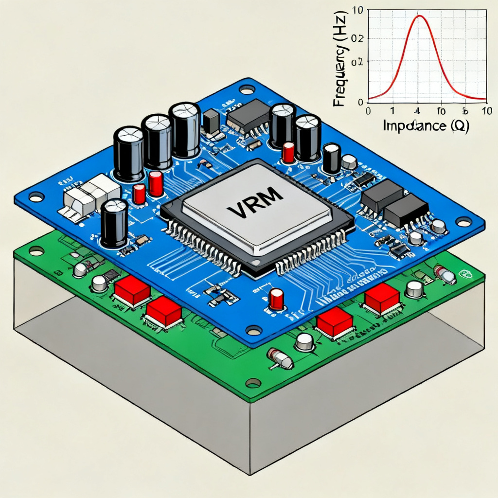
Simulation and Measurement Verification
AC Impedance Simulation
Use tools like Ansys SIwave or Cadence Sigrity to plot impedance vs. frequency. Key metrics: peak impedance (must be below Z_target) and resonance frequency (avoid peaks near clock harmonics).
Time-Domain Transient Simulation
Apply a current step (e.g., 0 to 3A in 1 ns) and measure voltage droop. Use a target droop of <5% of V_rail.
Measurement Techniques
VNA (Vector Network Analyzer): Measures PDN impedance from 1 MHz to 10 GHz. Requires 50-ohm reference and calibration. TDR (Time-Domain Reflectometry): Measures impedance vs. time (distance) along the PDN. Oscilloscope with low-inductance probe: Measures voltage ripple under dynamic load.
Tools and Resources for PDN Impedance Tuning
Recommended Simulation Tools
Ansys SIwave: Full-wave 3D solver for PDN and SI. Cadence Sigrity PowerSI: Fast AC and transient PDN simulation. Keysight ADS: For combined SI/PI simulation. Open-source tools: GNU Octave or Python with scikit-rf for basic modeling.
PCB Design Guidelines
Use IPC-2221 or JEDEC standards for capacitor selection. Refer to IC vendor PDN guidelines (e.g., Intel, Xilinx, Texas Instruments). For high-speed PCBs, follow the stackup recommendations from your PCB manufacturer (e.g., 4–8 layers, thin dielectric).
Frequently Asked Questions
What is PDN Impedance Tuning in high-speed PCB design?
PDN Impedance Tuning is the process of adjusting the power distribution network (PDN) components—such as VRMs, capacitors, PCB planes, and vias—to ensure the impedance remains below the target impedance across the operating frequency range, thereby maintaining power integrity.
How do I calculate target impedance for my PCB?
Target impedance is calculated using the formula: Z_target = (V_rail × Ripple_Tolerance) / I_transient. For example, a 1.8V rail with 5% ripple tolerance and 2A transient current yields 45 mΩ. This value must be maintained from DC to the highest frequency of interest for reliable PDN Impedance Tuning.
What are common mistakes in PDN Impedance Tuning?
Common pitfalls include overlooking VRM bandwidth, using too few decoupling capacitors, ignoring via inductance, poor capacitor placement, and not simulating the full PDN. Each can cause impedance peaks that degrade power integrity.
Which tools are best for PDN Impedance Tuning simulation?
Ansys SIwave, Cadence Sigrity PowerSI, and Keysight ADS are industry-standard for PDN Impedance Tuning. Open-source options like GNU Octave with scikit-rf are suitable for basic modeling.
How does via inductance affect PDN Impedance Tuning?
Via inductance adds 0.5–1 nH per via, causing high-frequency impedance peaks. Using multiple parallel vias (e.g., 4–8) and minimizing via length are key techniques in PDN Impedance Tuning to keep impedance below target.
Conclusion
PDN impedance tuning is a critical step in high-speed PCB design that directly impacts power integrity, signal integrity, and overall system reliability. By understanding the frequency-dependent behavior of VRMs, capacitors, planes, and vias, and by following a systematic tuning process—defining target impedance, modeling, selecting components, optimizing stackup, and simulating—you can achieve a PDN that stays below the target impedance across the entire frequency range. Advanced techniques like embedded capacitance and anti-resonance mitigation further enhance performance. With careful design and verification, you can ensure that your high-speed PCB delivers stable, noise-free power to even the most demanding ICs.
| Parameter | Value | Impact on PDN Impedance Tuning |
|---|---|---|
| V_rail | 1.8V | Determines Z_target |
| Ripple Tolerance | 5% | Affects target impedance calculation |
| I_transient | 2A | Sets current demand |
| Z_target | 45 mΩ | Maximum allowed impedance |
| VRM Output Impedance | 12 mΩ | Low-frequency limit |
| Bulk Capacitor ESR | 50 mΩ | Influences mid-frequency impedance |
| Decoupling Capacitor ESL | 0.5 nH | High-frequency performance |
| Via Inductance per Via | 0.5–1 nH | Causes high-frequency peaks |