How to design a Power Distribution Network for high-current processors is critical for maintaining voltage stability under transient loads exceeding 100A. A robust PDN ensures reliable processor operation by minimizing impedance from DC to gigahertz frequencies, preventing voltage droop and signal integrity degradation.
This pillar content provides a step-by-step, engineer-level guide to designing a robust PDN for high-current processors, covering impedance planning, decoupling strategies, PCB stack-up, via optimization, and simulation validation.
1. Understanding PDN Impedance Target and Frequency Range for High-Current Processors
The fundamental goal of a Power Distribution Network is to maintain the supply voltage within a tight tolerance (e.g., ±3% to ±5%) across all transient current demands. This is achieved by keeping the PDN impedance below a target value across the frequency range of interest (typically DC to several hundred MHz or even GHz).
1.1 Calculating the Target Impedance for Power Distribution Network Design
The classic formula for target impedance \( Z_{target} \) is:
\( Z_{target} = \frac{V_{DD} \times \text{Tolerance}}{\Delta I_{max}} \)
Where:
- \( V_{DD} \) = Core voltage (e.g., 1.0V)
- Tolerance = Allowed ripple (e.g., 3% = 0.03V)
- \( \Delta I_{max} \) = Maximum transient current step (e.g., 50A)
Example: For a 1.0V processor with 3% tolerance and a 50A transient, \( Z_{target} = \frac{0.03}{50} = 0.6 m\Omega \). This is an extremely low impedance target, requiring careful design.
Important nuance: Modern processors often have multiple supply domains (core, I/O, memory, PLL) with different current profiles and impedance requirements. Each domain must be analyzed separately.
1.2 Frequency Range of Interest in Power Distribution Network
The PDN must maintain low impedance from DC up to the highest harmonic frequency of the processor’s switching activity. For a 2GHz processor, the relevant frequency range extends to at least 2GHz (or even 5th harmonic = 10GHz for very fast edges). This dictates the need for multiple decoupling stages.
2. The Four-Stage Decoupling Strategy for Power Distribution Network
No single capacitor type or placement can cover the entire frequency range. A successful Power Distribution Network uses a hierarchical decoupling strategy with four distinct stages:
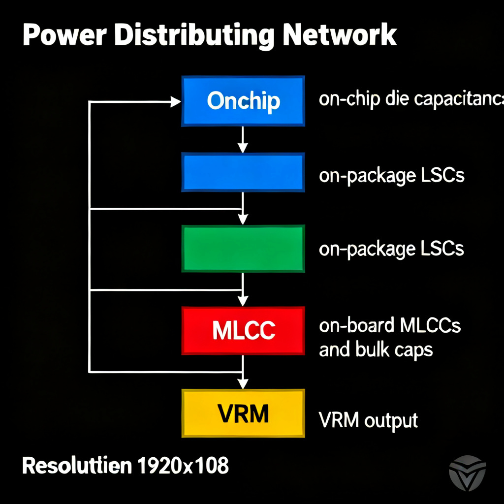
Stage 1: On-Chip Decoupling (Die-Level)
On-chip decoupling operates above 100 MHz to GHz, using on-die capacitance (MOSFET gate capacitance, MIM capacitors). It provides the first response to fast current transients before off-chip capacitors can react. The die capacitance is typically in the range of tens to hundreds of nF. You cannot change this, but you must account for it when modeling the PDN. The on-chip capacitance sets the high-frequency impedance floor.
Stage 2: On-Package Decoupling (Substrate-Level)
On-package decoupling covers 10 MHz to 100 MHz using land-side capacitors (LSCs) and package substrate capacitors (e.g., MLCCs with low ESL, typically 0201 or 0402 size). Place them as close as possible to the processor bumps or balls, often directly under the die on the bottom side of the package substrate. Use capacitance values of 0.1 µF to 10 µF per capacitor, with low ESL (< 0.2 nH). Critical rule: Use multiple small-value capacitors in parallel to reduce ESL and ESR, not a single large-value cap.
Stage 3: On-Board Decoupling (PCB-Level)
On-board decoupling covers 100 kHz to 10 MHz using bulk capacitors (tantalum, polymer, or aluminum electrolytic) and ceramic capacitors (MLCCs, e.g., 10 µF, 22 µF, 47 µF in 0805 or 1206 packages). Place them within 1-2 inches of the processor power pins, on the same layer as the power plane or via a short, wide trace. This stage handles mid-frequency transients and provides local energy storage. Important: The resonant frequency of these capacitors must be carefully chosen to avoid anti-resonance with the plane capacitance.
Stage 4: VRM and Bulk Capacitance
VRM and bulk capacitance covers DC to 100 kHz using VRM output capacitors (bulk electrolytic, e.g., 470 µF to 4700 µF) and the VRM itself. Place them at the VRM output, typically several inches from the processor. This stage provides the steady-state current and handles low-frequency load changes. Note: The VRM has a finite bandwidth (typically 10-100 kHz). Above this frequency, the VRM is effectively an open circuit, and the decoupling capacitors must take over.
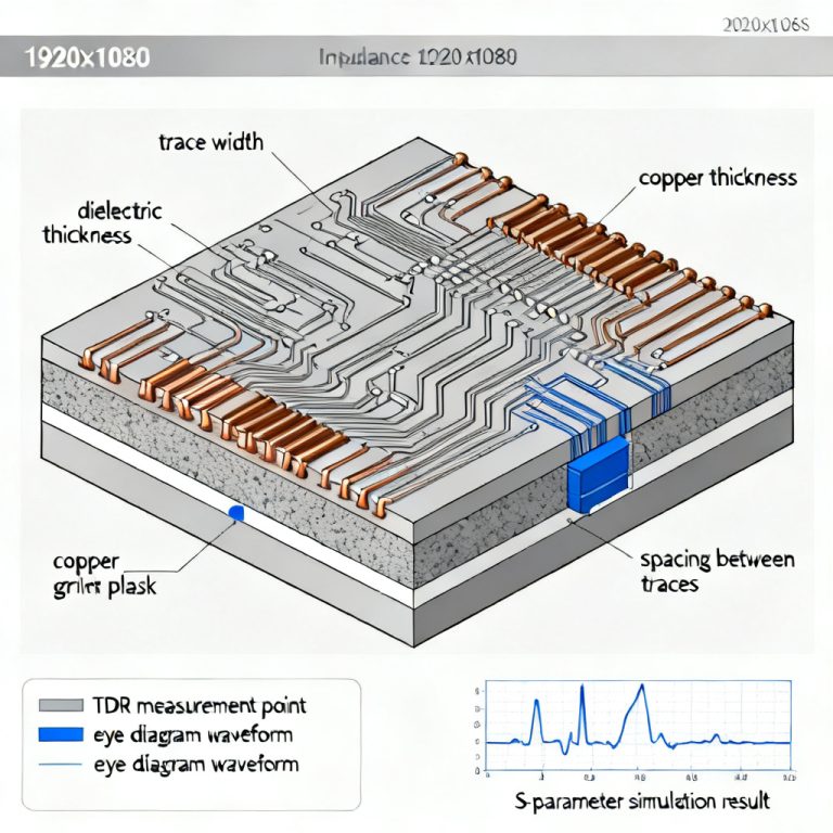
3. PCB Stack-Up Design for Low Inductance in Power Distribution Network
The PCB stack-up is the foundation of a low-impedance PDN and plays a vital role in Power Integrity PCB. For high-current processors, a dedicated power-ground plane pair is mandatory.
3.1 Plane Capacitance for Power Distribution Network
A power plane and ground plane separated by a thin dielectric form a distributed capacitor. This provides very low ESL and ESR at high frequencies (above 10-100 MHz). Use the thinnest possible prepreg (e.g., 2 mil or 50 µm) between the power and ground plane pair. Thinner dielectric increases plane capacitance per square inch. Keep the plane pair as close as possible (e.g., Layer 2 = GND, Layer 3 = VDD, with a 2-mil core). For a 2-mil FR4 dielectric, capacitance is roughly 200 pF per square inch. A 10-inch square plane provides about 2 nF of distributed capacitance.
3.2 Plane Inductance in Power Distribution Network
The loop inductance of the power-ground plane pair is critical. It is proportional to the separation distance. For a 2-mil separation, loop inductance is approximately 0.1 nH per square inch. For 10-mil separation, it rises to 0.5 nH per square inch. Keep the planes as close as possible.
3.3 Multiple Plane Pairs for Power Distribution Network
For processors with multiple voltage domains (e.g., VDD_CORE, VDD_IO, VDD_MEM), use dedicated plane pairs for each domain. Do not share planes between noisy and sensitive domains. Use split planes or moats, but ensure that high-frequency return currents are not interrupted. If split planes are used, provide stitching capacitors across the split.
4. Via Optimization and Current Path Design for Power Distribution Network
Vias are a major source of inductance and resistance in the PDN. Poor via design can negate the benefits of low-inductance planes.
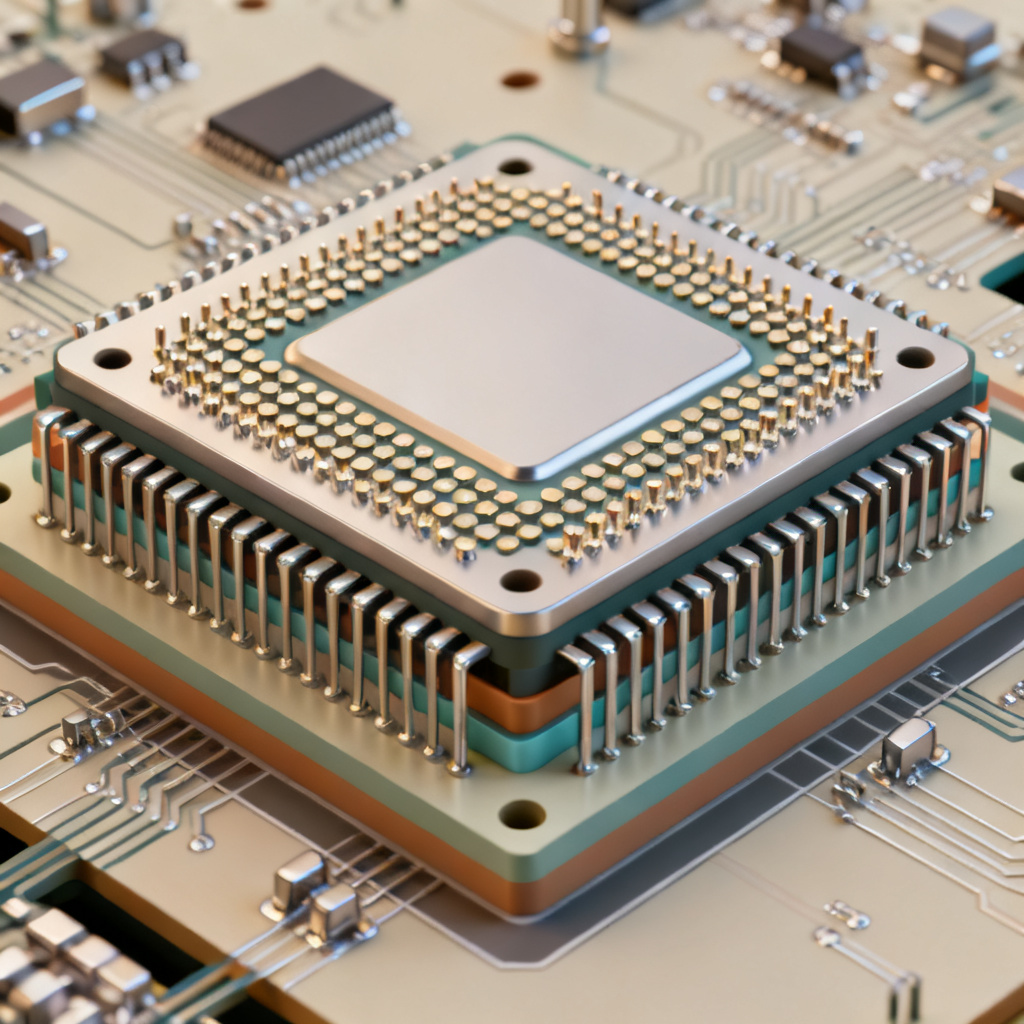
4.1 Via Inductance in Power Distribution Network
A standard via (10 mil drill, 20 mil pad) has approximately 1 nH of inductance per millimeter of length. Reduction techniques: Use multiple vias in parallel (4-8 vias per power pin), place ground vias adjacent to power vias to create a low-inductance loop, use larger via diameters (20-mil vs 8-mil), and avoid long via stubs by back-drilling.
4.2 Via Resistance and Current Handling in Power Distribution Network
High current (e.g., 100A) requires sufficient copper cross-section. A standard 10-mil via with 1 oz copper can handle about 1-2A (depending on temperature rise). For 100A, you need at least 50-100 vias in parallel. Arrange vias in a grid or array under the processor footprint. Use thermal relief spokes only if necessary; solid connections to the plane are better for low resistance.
4.3 Via Stitching for Plane Pairs in Power Distribution Network
Connect the power and ground planes to each other at multiple points around the PCB perimeter and near the processor. This reduces the resonant cavity modes and lowers impedance at high frequencies. Place stitching vias every 1/20th of the wavelength of the highest frequency of interest. For 2 GHz, the wavelength in FR4 is about 3.5 inches; stitching every 0.175 inches is ideal.
5. Capacitor Selection and Placement Optimization for Power Distribution Network
5.1 Capacitor Type and Value Selection for Power Distribution Network
Use MLCCs (Class II, e.g., X7R, X5R) for mid-frequency (100 kHz – 10 MHz) with values like 0.1 µF, 1 µF, 10 µF, 22 µF. Note that DC bias can reduce capacitance by up to 80% for high-K dielectrics. Derate by 50% for 1V operation. Use low-ESL capacitors (reverse-geometry 0612, 0508 or interdigitated IDC) for lower ESL (0.1-0.2 nH vs 0.5-1 nH for standard 0805). Use polymer tantalum (e.g., 100 µF, 330 µF) or aluminum polymer for low-frequency (DC – 100 kHz). Avoid using only one value of capacitor; a range of values (e.g., 0.1 µF, 1 µF, 10 µF, 100 µF) covers a broader frequency spectrum.
5.2 Anti-Resonance and Damping in Power Distribution Network
When multiple capacitor types are used in parallel, their combined impedance can create an anti-resonance peak (a high-impedance spike) at the frequency where the inductance of one cap resonates with the capacitance of another. Mitigation: Use capacitors with similar ESL values, add a small amount of resistance (e.g., 0.1-0.5 ohms) in series with some bulk capacitors to dampen the resonance, and use a simulated impedance profile to identify and reduce anti-resonance peaks.
5.3 Placement Rules for Power Distribution Network Capacitors
Place the smallest, fastest capacitors closest to the processor power pins. The loop inductance from capacitor to processor pin is proportional to the distance. Place the capacitor’s vias as close to the capacitor pads as possible. Use two vias per capacitor (one for power, one for ground) to minimize loop area. For high-frequency capacitors (e.g., 0.1 µF), spread them evenly around the processor footprint. For bulk capacitors, cluster them near the VRM output. Use the widest possible traces (or direct plane connection) from capacitor pads to vias. Avoid long, narrow traces.
6. Simulation and Verification of Power Distribution Network
Designing a PDN without simulation is guesswork. Use the following tools and methods:
6.1 DC IR Drop Analysis for Power Distribution Network
Ensure that the DC resistance (DCR) of the PDN does not cause excessive voltage drop (e.g., > 20 mV for a 1V rail). Use tools like Ansys SIwave, Cadence Sigrity, or free tools like KiCad’s IR drop simulation. Input full PCB stack-up, copper thickness, via parameters, current draw per pin. Output a voltage contour map showing hot spots. Redesign if drop exceeds tolerance.
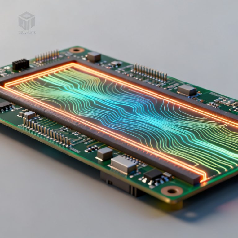
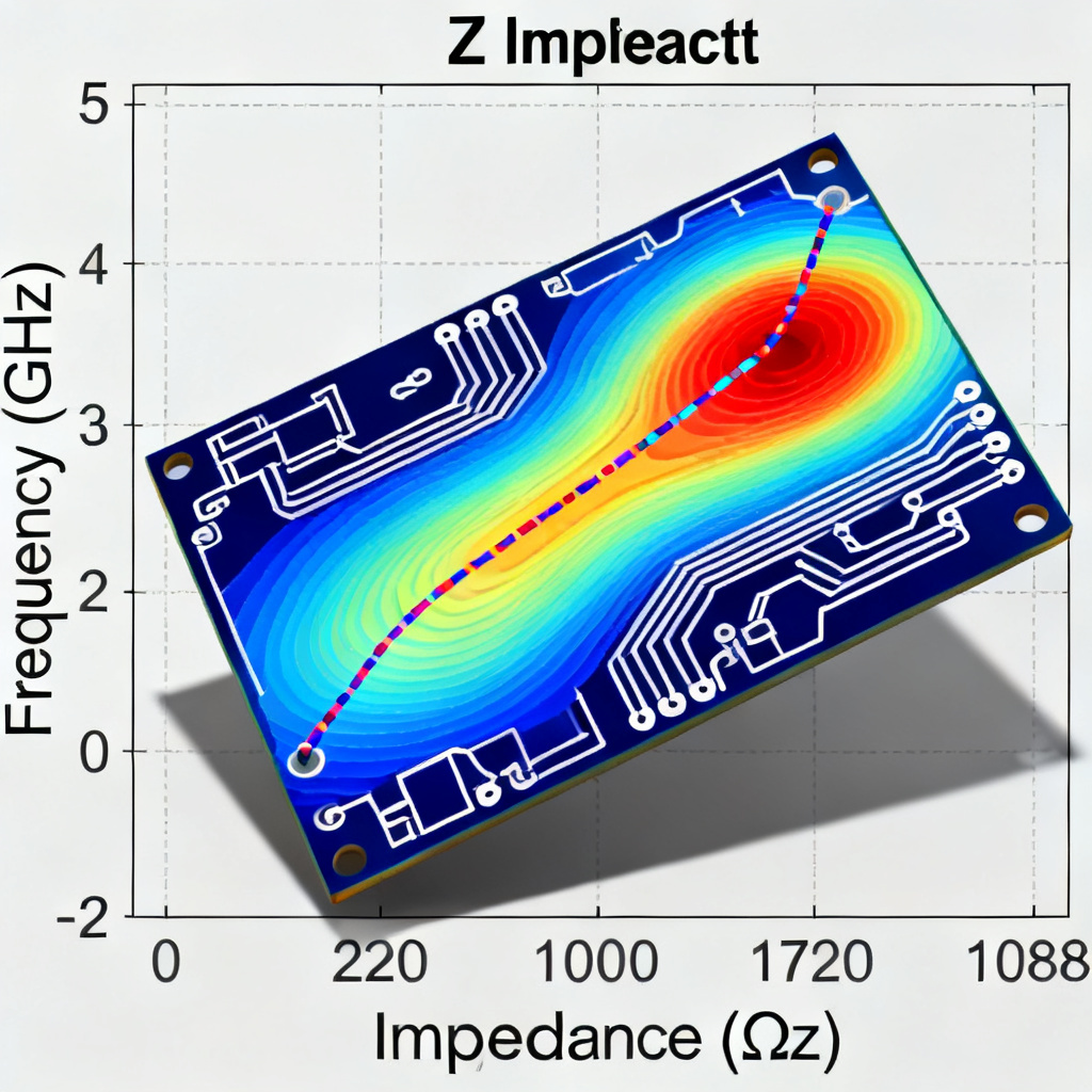
6.2 AC Impedance Simulation (Z-Profile) for Power Distribution Network
Verify that the PDN impedance stays below \( Z_{target} \) across the frequency range. Use tools like Ansys SIwave, Cadence Sigrity, Keysight ADS, or CST. Inject an AC current source at the processor power pins and sweep frequency from DC to 10 GHz. Plot impedance magnitude. The impedance curve should be flat and below \( Z_{target} \). Any peaks above \( Z_{target} \) indicate a resonance issue.
6.3 Transient Simulation for Power Distribution Network
Simulate the processor’s current step (e.g., from 10A to 100A in 1 ns) and observe the voltage response. Use SPICE-based tools (e.g., LTspice with extracted PDN model). Voltage droop should not exceed the specified tolerance (e.g., 30 mV for a 1V rail). Overshoot and ringing should be minimal.
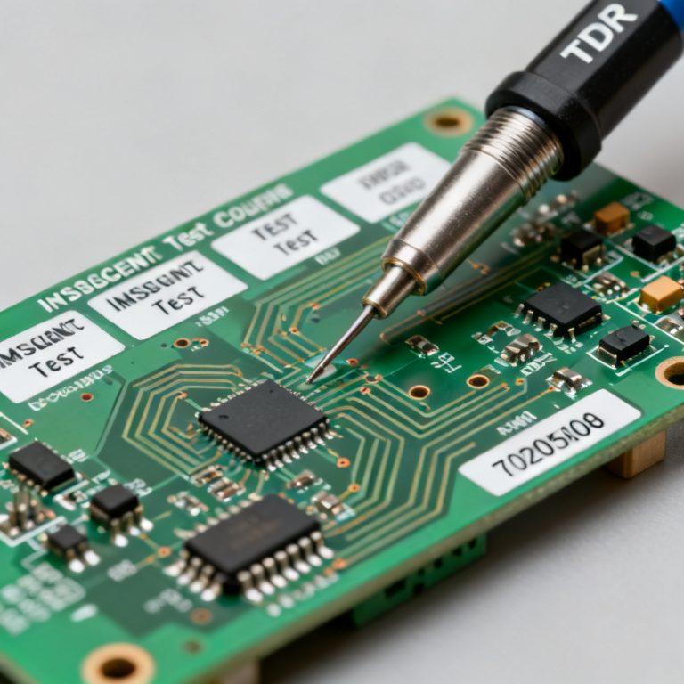
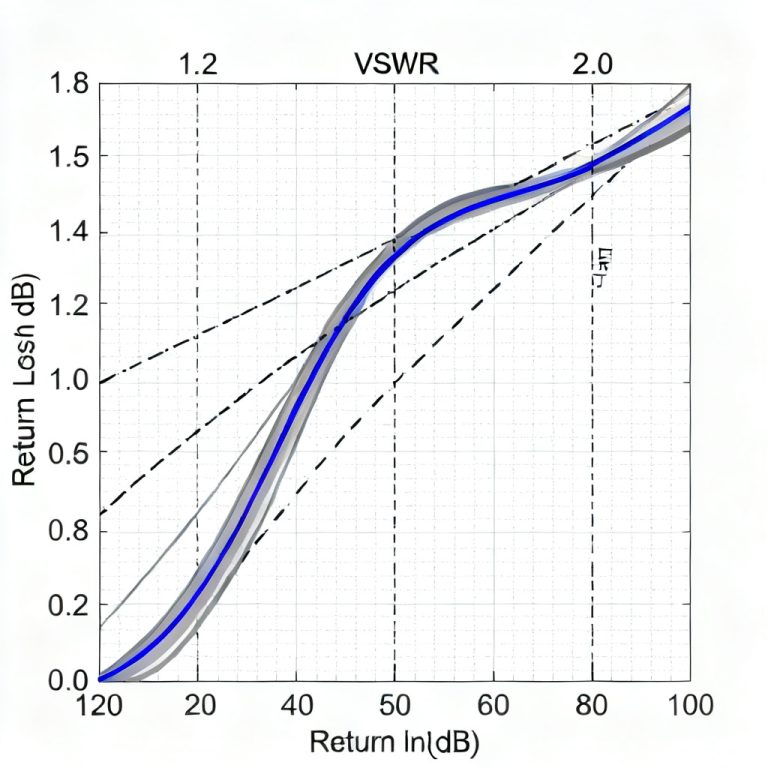
6.4 Measurement Correlation for Power Distribution Network
After prototype, measure the PDN impedance using a Vector Network Analyzer (VNA) or impedance analyzer. Compare to simulation to validate the model.
7. Thermal Management and High-Current Routing for Power Distribution Network
High current generates heat. The PDN design must consider thermal effects. Use 2 oz or even 3 oz copper on power planes for high-current rails. This reduces resistive losses and heat generation. Use arrays of thermal vias under the processor to conduct heat to inner ground planes. Ensure that trace widths and via counts are sufficient to keep current density below 10 A/mm² (or per IPC-2221 standards). For example, a 100A rail requires a 10 mm wide trace on 1 oz copper (or multiple parallel traces).
8. Common Pitfalls and How to Avoid Them in Power Distribution Network Design
| Pitfall | Consequence | Solution |
|---|---|---|
| Too few vias under processor | High via inductance, voltage droop | Use 8-16 vias per power pin |
| Capacitor placed far from load | Increased loop inductance, reduced effectiveness | Place smallest caps within 100 mils of pins |
| Using only one capacitor value | Narrow frequency coverage, anti-resonance | Use a range of values (0.1 µF to 100 µF) |
| Ignoring DC bias effect on MLCCs | Actual capacitance 50-80% lower than nominal | Derate capacitance by 50% for 1V rails |
| Thin power plane (1 oz) for 100A | Excessive IR drop, overheating | Use 2 oz or 3 oz copper on power layers |
| No plane pair under processor | High loop inductance, poor high-frequency PDN | Dedicate a power-ground plane pair directly under the processor |
9. Design Workflow Summary for Power Distribution Network
- Define requirements: Voltage, current, tolerance, transient step size for each rail.
- Calculate target impedance for each domain.
- Select decoupling strategy: On-chip, on-package, on-board, VRM.
- Design PCB stack-up: Thin dielectric plane pair, dedicated layers for each domain.
- Optimize via placement: Multiple vias per pin, ground vias adjacent to power vias.
- Select and place capacitors: Use a range of values, smallest closest to load.
- Simulate DC IR drop and AC impedance: Iterate until below target.
- Simulate transient response: Ensure voltage tolerance is met.
- Validate with measurement on prototype.
- Document the PDN design for future reference and manufacturing.
10. Frequently Asked Questions About Power Distribution Network Design
What is the target impedance for a Power Distribution Network in high-current processors?
The target impedance for a Power Distribution Network is calculated using \( Z_{target} = \frac{V_{DD} \times \text{Tolerance}}{\Delta I_{max}} \). For a 1.0V processor with 3% tolerance and 50A transient, the target is 0.6 mΩ.
How does PCB stack-up affect Power Distribution Network performance?
A thin dielectric layer between power and ground planes in the Power Distribution Network reduces loop inductance and increases distributed capacitance, improving high-frequency performance.
Why is via optimization important in Power Distribution Network design?
Vias introduce inductance and resistance in the Power Distribution Network. Using multiple parallel vias and placing ground vias adjacent to power vias minimizes loop inductance and ensures stable voltage delivery.
Conclusion
Designing a PDN for high-current processors is a multi-disciplinary challenge requiring knowledge of electromagnetic theory, capacitor behavior, PCB manufacturing, and thermal management. The key takeaways are:
– Impedance target is the single most important specification.
– Hierarchical decoupling from die to VRM covers the full frequency range.
– Low-inductance planes and vias are critical for high-frequency performance.
– Simulation is non-negotiable—verify before building.
– Thermal and current density must be considered for reliability.
By following this guide, you can create a Power Distribution Network that delivers clean, stable power to even the most demanding processors, ensuring reliable operation in high-speed, high-current applications.