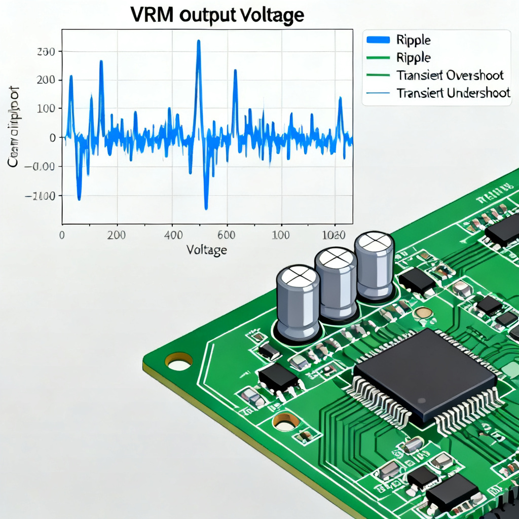
In high-speed PCB design, Switching Noise from VRM Output acts as a dominant factor affecting PCB power integrity. Generated by the switching operations of Voltage Regulator Modules (VRM), this type of noise directly endangers overall system stability and signal quality.
Causes and Characteristics of VRM Switching Noise
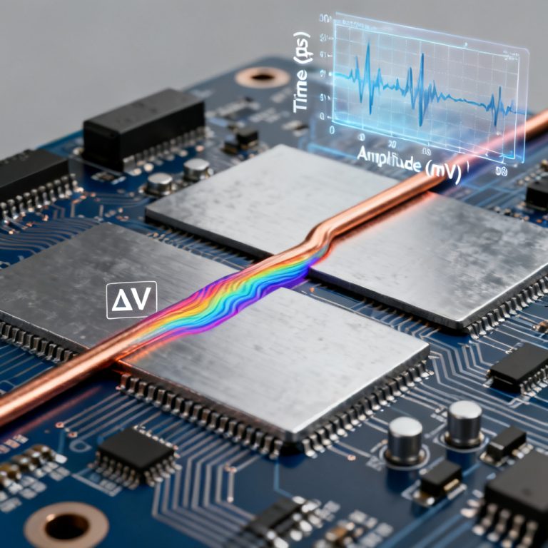
VRMs employ pulse-width modulation to drive switching transistors, which generates voltage ripples, transient response noise and high-frequency harmonics. Covering a frequency band from 100 kHz to megahertz range, Switching Noise from VRM Output severely impairs power integrity performance of PCBs. Even a 10 mV ripple can induce logic faults in contemporary high-speed circuit designs.
Voltage Ripple and Transient Response
Voltage ripples are mainly caused by the equivalent series resistance (ESR) and equivalent series inductance (ESL) of output capacitors. When load current changes drastically, the inherent delay of the VRM feedback loop produces transient response noise. These two components constitute the main part of Switching Noise from VRM Output.
High-Frequency Harmonics
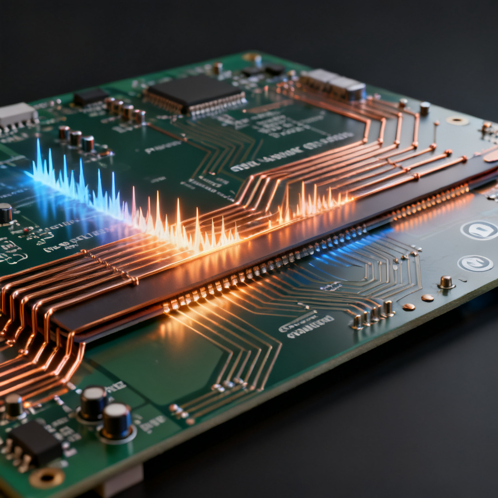
Parasitic inductance at switching nodes triggers ringing with frequencies reaching tens of megahertz. This noise propagates to sensitive circuits through the power distribution network (PDN), further raising the difficulty of power integrity PCB design.
Impact on Power Integrity PCB
Transmitted across the PDN, Switching Noise from VRM Output brings about reduced voltage margin, degraded signal integrity and electromagnetic interference (EMI) issues. Taking DDR4 design as an example, a 20 mV ripple will lead to a notable rise in timing jitter.
Voltage Margin Reduction
Most modern integrated circuits feature a power supply tolerance of ±3% to ±5%, and Switching Noise from VRM Output will consume part of this tolerance budget. Therefore, effective control over this noise is the core to guarantee sufficient voltage margin for PCBs.
Signal Integrity Degradation
Power noise couples into signal traces and gives rise to crosstalk and narrowed eye diagrams. For high-speed SerDes links, merely 10 mV of Switching Noise from VRM Output can increase the bit error rate (BER) by an order of magnitude.
Mitigation Strategies for VRM Noise
Reasonably designed decoupling capacitor networks, optimized PCB layout and stackup, together with simulation verification, can effectively suppress Switching Noise from VRM Output and improve the robustness of power integrity on PCBs.
Decoupling Capacitor Network
Adopt a combination of capacitors with different capacitance values. Large electrolytic capacitors suppress low-frequency ripples, conventional ceramic capacitors mitigate mid-to-high frequency noise, and MLCCs are used to eliminate ringing. Place decoupling components close to VRM output pins and route with short and wide traces.
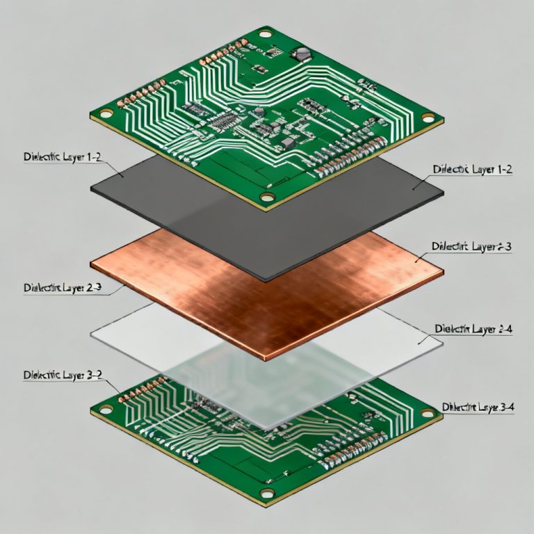
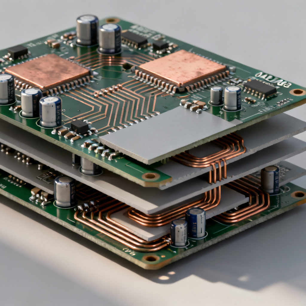
PCB Stackup and Layout Optimization
Deploy complete power and ground planes, and keep the plane spacing within 4 mils to form low-impedance planar capacitance. Isolate sensitive circuits with guard traces or ground islands. Use no less than four parallel vias to lower inductance.
PDN Analysis Simulation Tools
Industry-standard tools including Ansys SIwave, Cadence Sigrity and Keysight ADS are used for PDN impedance analysis and time-domain transient simulation. The formula for target impedance is shown below:
Ztarget=ΔIloadVout×Ripple Percentage
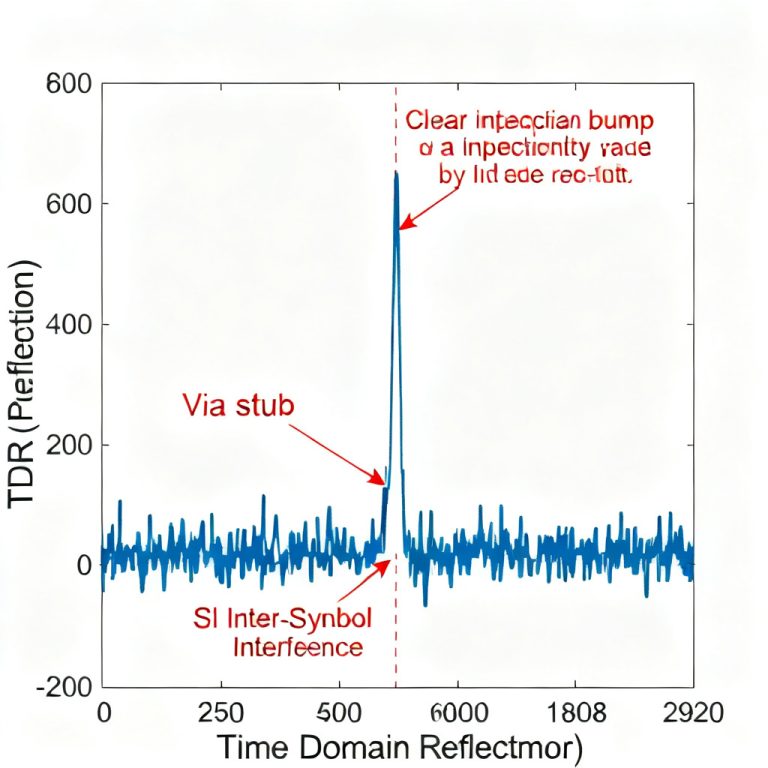
Real-World Case Study
A 12-layer high-speed FPGA board is used for verification. Its core supply voltage is 1.0 V, and the voltage undershoot reaches 80 mV under sudden load changes. After optimizing decoupling capacitor placement and power plane spacing, the PDN impedance is reduced to 5 mΩ, and the undershoot caused by Switching Noise from VRM Output drops to 35 mV.
Industry Best Practices
- Define PDN target impedance in the early design phase.
- Follow the standard configuration: match 1 μF, 0.1 μF and 0.01 μF capacitors for every 100 mA load current.
- Implement simulation-driven design throughout the whole process.
- Select oscilloscopes with a bandwidth of 500 MHz or higher for testing.
- Save PDN impedance curves for reference in subsequent projects.
Frequently Asked Questions
What is Switching Noise from VRM Output?
How does VRM noise affect Power Integrity PCB?
What are effective mitigation techniques for VRM switching noise?
| Technique | Key Parameters | Impact on Power Integrity PCB |
|---|---|---|
| Decoupling Capacitors | ESR < 10 mΩ, ESL < 1 nH | Reduces ripple by 40-60% |
| Power Plane Optimization | Spacing ≤ 4 mil | Lowers PDN impedance by 30% |
| Ferrite Beads | DCR < 50 mΩ, frequency 10-100 MHz | Suppresses high-frequency noise |