Mastering power integrity PCB design for FPGA and ASIC power delivery is the foundation of reliable high-speed systems. This guide synthesizes top industry knowledge to provide a complete, step-by-step approach for designing a robust power distribution network (PDN).
Understanding the Power Delivery Network and Its Challenges
The Fundamental Goal of a PDN
The primary function of a power delivery network (PDN) is to deliver a stable voltage with minimal ripple and noise to every active device on the board. For FPGAs and ASICs, this means maintaining the core voltage (Vcore) within a tight tolerance—typically ±3% or ±5%—even during rapid transient current changes. The PDN must act as a low-impedance path from the voltage regulator module (VRM) to the die. This is the essence of power integrity PCB design.
The Impedance Target: The Z-Target Curve
The most critical metric in PDN design is the target impedance (Z_target). This is the maximum impedance the PDN can present to the device across a wide frequency range (DC to several GHz). The formula is:
Z_target = (V_core × Tolerance) / ΔI_transient
For example, a 1.0V core with a 3% tolerance and a 10A transient step requires a target impedance of 3 mΩ. Achieving sub-10 mΩ impedance up to 100 MHz or higher is a common challenge. The PDN impedance curve must remain below this target across all frequencies to prevent voltage droop and overshoot.
The Frequency Domain Problem
The PDN is not a simple DC path. It exhibits frequency-dependent behavior due to parasitic inductance and capacitance. The impedance profile of a typical PDN has three distinct regions:
– Low Frequency (DC to ~1 kHz): Dominated by the VRM output impedance and bulk capacitance.
– Mid Frequency (~1 kHz to ~1 MHz): Controlled by bulk electrolytic and ceramic capacitors.
– High Frequency (~1 MHz to >1 GHz): Governed by high-frequency MLCCs, on-die capacitance, and the PCB plane inductance.
The challenge is to ensure a smooth transition between these regions without creating impedance peaks that violate the Z_target.
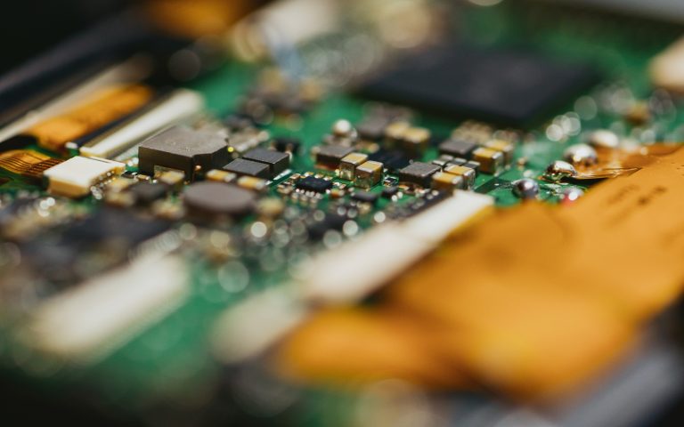
Decoupling Capacitor Strategy: The Art of the Decap
The Role of Capacitors in the PDN
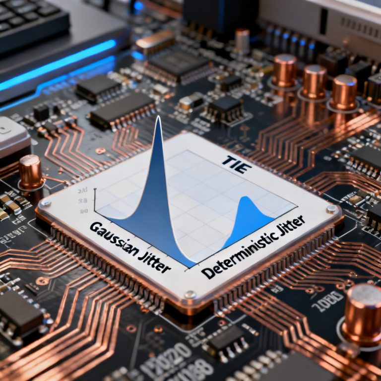
Decoupling capacitors (decap) are the primary tool for lowering PDN impedance. They act as local energy reservoirs, providing instantaneous current to the device when the VRM cannot respond fast enough. Each capacitor has a self-resonant frequency (SRF) above which it becomes inductive. Therefore, multiple capacitor values and packages are required to cover the full frequency range.
Capacitor Selection: ESL, ESR, and SRF
– Equivalent Series Inductance (ESL): The single most important parasitic. A lower ESL shifts the SRF higher. Use small package sizes (0402, 0201) and low-inductance terminations (e.g., reverse-geometry or interdigitated capacitors) for high-frequency decoupling.
– Equivalent Series Resistance (ESR): Controls the damping of the resonance. Low ESR is good for high-frequency but can cause anti-resonance peaks. A mix of low and moderate ESR capacitors is recommended.
– Self-Resonant Frequency (SRF): The frequency where the capacitor’s impedance is minimal. For example, a 100nF 0402 ceramic capacitor typically has an SRF around 10-20 MHz, while a 10pF 0201 can reach above 1 GHz.
The Ten Decade Rule and Bypass Network
A robust decoupling strategy follows the “ten decade” rule: use capacitors that are spaced roughly one decade apart in value (e.g., 10µF, 1µF, 0.1µF, 10nF, 1nF). However, modern FPGA and ASIC designs require more precision. A better approach is:
– Bulk Capacitors (10-100 µF): Tantalum or aluminum polymer. Placed near VRM output. Handle low-frequency transients.
– Mid-Frequency Capacitors (0.1-1 µF): X7R ceramic MLCCs. Placed near the periphery of the FPGA/ASIC.
– High-Frequency Capacitors (0.01-0.1 µF): NP0/C0G or X7R in 0402/0201. Placed directly on the bottom side (if BGA) or within 50 mils of the power pins.
– Ultra-High-Frequency Capacitors (1-100 pF): NP0/C0G in 0201 or 01005. Used for decoupling at >1 GHz. Often placed inside the BGA footprint.
Anti-Resonance: The Silent Killer
When two capacitors of different values are placed in parallel, their individual impedance curves can combine to create a parallel resonance peak where the impedance spikes above the target. This occurs at the frequency where one capacitor is inductive and the other is capacitive. To mitigate:
– Use capacitors with similar ESR to dampen the peak.
– Add a small amount of lossy capacitance (e.g., a higher ESR tantalum) in the mid-frequency range.
– Simulate the combined impedance profile before layout.
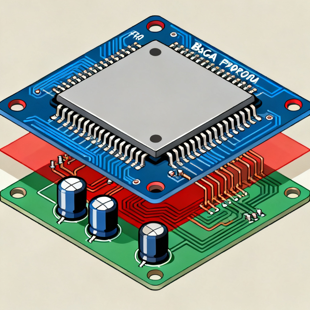
PCB Stack-Up and Plane Design for Low Impedance
The Importance of Power/Ground Planes
A solid, continuous power plane and ground plane are the foundation of any high-performance PDN. They provide:
– Low Inductance: A plane pair (power and ground) acts as a distributed capacitor with extremely low inductance (typically < 1 pH per square).
– Shielding: Planes isolate signal layers and reduce EMI.
– Return Path: They provide a consistent low-inductance return path for high-speed signals.
Plane Capacitance: The Built-In Decap
The capacitance between a power plane and an adjacent ground plane (C_plane) is given by:
C_plane = (ε_r × ε_0 × A) / d
Where d is the dielectric thickness. To maximize this capacitance, use a thin dielectric (e.g., 2-4 mils) between the power and ground plane pair. This is often called a “thin-core” or “close-coupled” stack-up. A 2-mil prepreg (e.g., 1080 or 106) can provide 100-200 pF per square inch, which is effective for decoupling above 100 MHz.
Recommended Stack-Up for High-Speed FPGA/ASIC
A typical 8-layer stack-up optimized for PDN is:
1. Top Layer: Signal (microstrip)
2. Layer 2: Ground (continuous)
3. Layer 3: Power (e.g., Vcore) – thin dielectric to Layer 2
4. Layer 4: Signal (stripline)
5. Layer 5: Signal (stripline)
6. Layer 6: Ground (continuous)
7. Layer 7: Power (e.g., VIO) – thin dielectric to Layer 6
8. Bottom Layer: Signal (microstrip)
Key: Layers 2-3 and 6-7 form close-coupled plane pairs. All power planes should be split only as a last resort; use islands or slots carefully.
Plane Splitting and Via Stitching
Avoid splitting the power plane under the FPGA/ASIC. If multiple voltages are required, use a dedicated plane layer for each major voltage (e.g., Vcore, VIO, Vaux). If a split is unavoidable (e.g., analog/digital), place a stitching capacitor across the split to provide a high-frequency return path. Every power via should have an adjacent ground via to minimize loop inductance.
Via Design and Layout Optimization
Via Inductance: The Bottleneck
Vias connecting the capacitor to the power plane are a major source of inductance. A standard 8-mil via (0.2mm) with a 20-mil pad has approximately 1-2 nH of inductance. This inductance can shift the effective SRF of a capacitor downward by a factor of 2-3. For example, a 100nF capacitor with 1 nH via inductance has an effective SRF of only ~10 MHz instead of 20 MHz.
Reducing Via Inductance
– Use multiple vias: For each capacitor, use at least two vias connecting to the power plane and two to the ground plane. Four vias are better.
– Minimize via length: The inductance is proportional to the via length. Use blind or buried vias if possible. A via from the top layer to the first internal plane is much shorter than one going through the entire board.
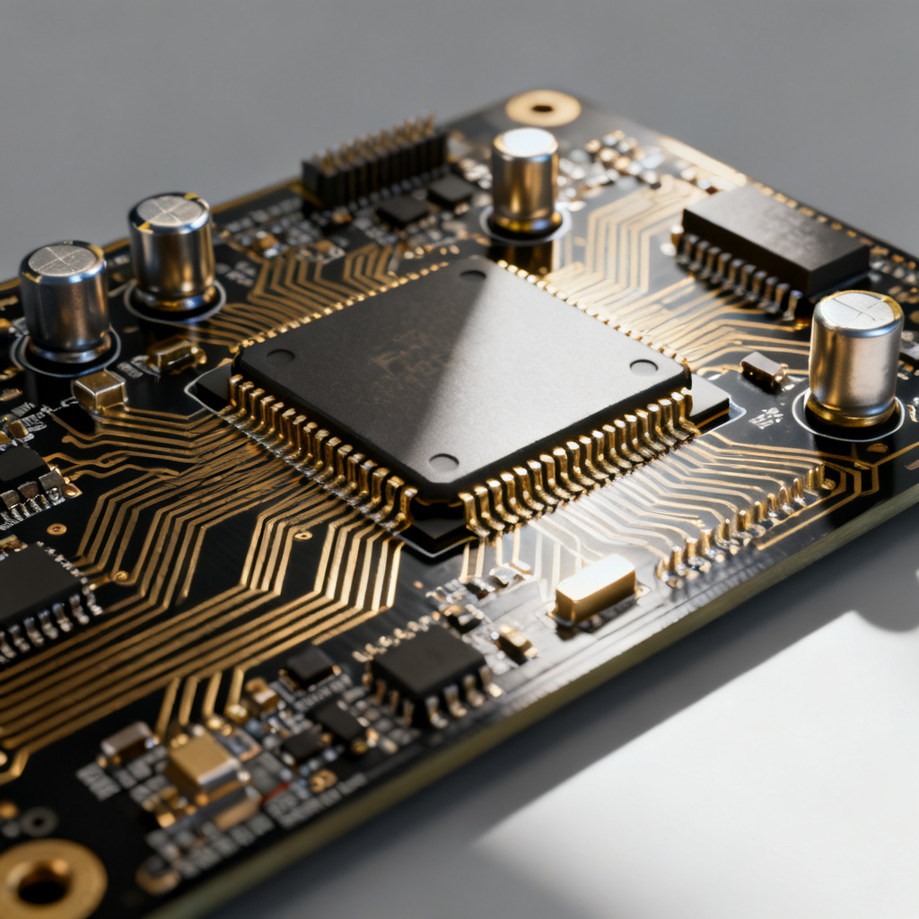
– Via-in-pad: For the FPGA/ASIC itself, use via-in-pad technology to connect the BGA balls directly to the internal planes. This eliminates the stub inductance of a via barrel.
– Ground via proximity: Place a ground via within 20 mils of every power via to create a low-inductance loop.
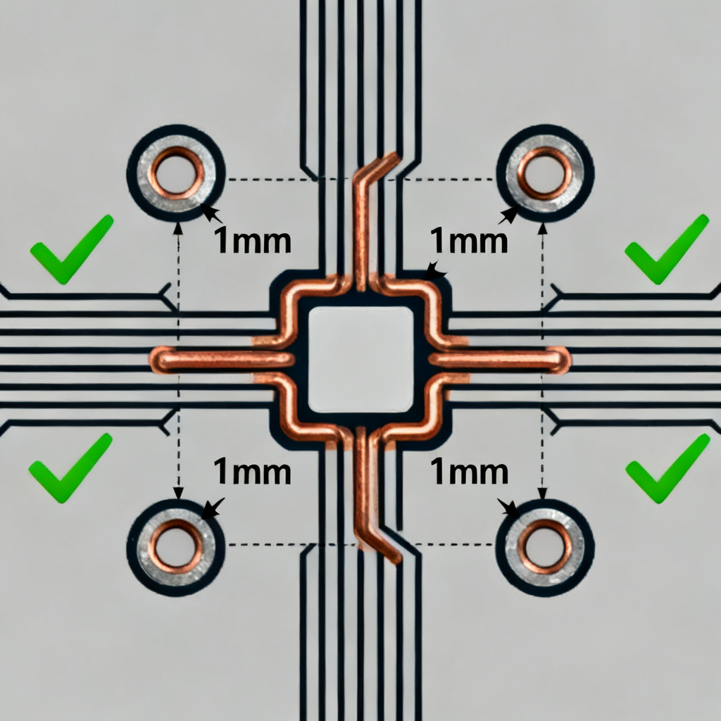
Capacitor Placement Rules
– Distance from FPGA: The high-frequency decoupling capacitors (0.1µF and below) must be placed within 50 mils (1.27 mm) of the FPGA power pins. For BGA devices, place them on the bottom side directly under the BGA footprint.
– Orientation: Orient capacitors such that their current loop (from pad to via to plane) is as short as possible. Avoid long traces; use a via directly at the capacitor pad.
– Grouping: Group capacitors by value and place them in a ring around the FPGA. The smallest values should be closest to the die.
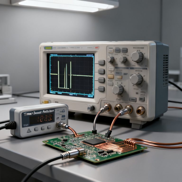
Simulation and Measurement Verification
Why Simulation is Mandatory
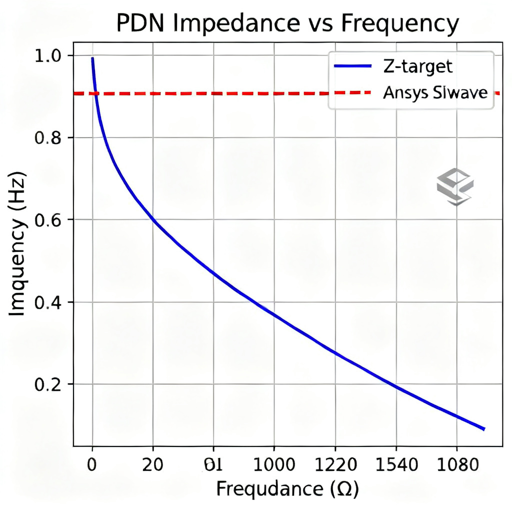
Modern FPGA and ASIC designs with sub-10 mΩ targets cannot be designed by rules of thumb alone. Simulation is essential to predict impedance peaks, resonance, and transient response before fabrication. Tools like Ansys SIwave, Cadence Sigrity, Keysight ADS, or Altium PDN Analyzer are industry standards.
Key Simulation Types
– AC Impedance Analysis (Z-parameter): Simulate the PDN impedance from the VRM to the die. Identify peaks above Z_target. This is the most critical simulation.
– Transient Analysis: Inject a step current (e.g., 10A in 1 ns) at the die and observe the voltage ripple. This validates the AC analysis.
– DC Drop Analysis (IR Drop): Simulate the DC voltage drop across the plane and via network. Ensure the total drop is within the tolerance (e.g., < 30 mV for a 1.0V core).
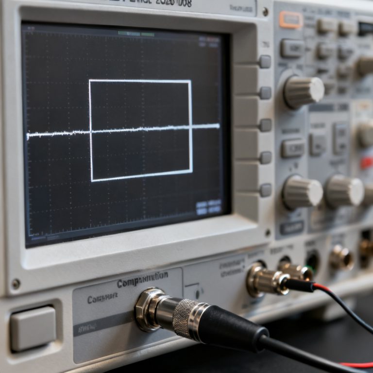
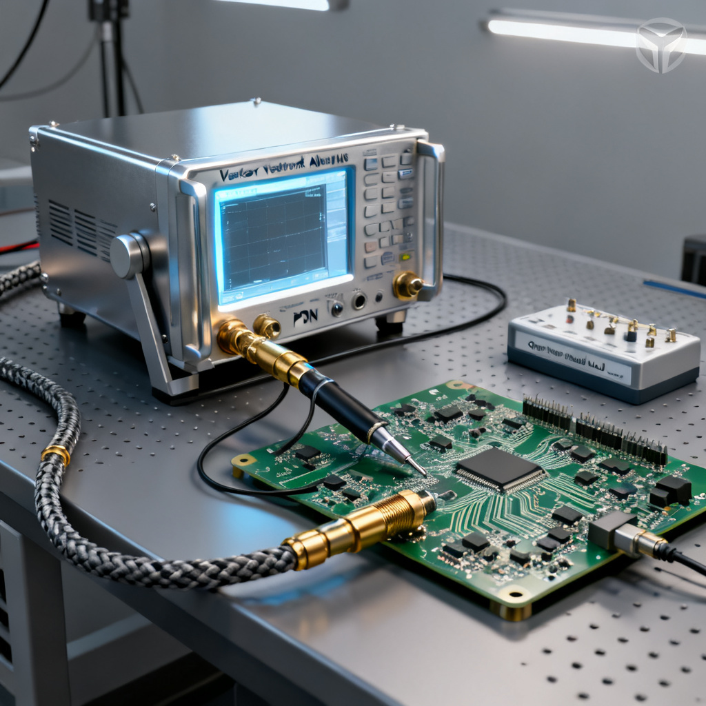
Measurement Techniques
– Vector Network Analyzer (VNA): The gold standard for measuring PDN impedance. Use a 2-port shunt-through measurement with a calibrated test fixture.
– Oscilloscope with Differential Probe: Measure voltage ripple at the FPGA core. Use a 1 GHz bandwidth probe and a low-noise oscilloscope.
– Time Domain Reflectometry (TDR): Useful for identifying impedance discontinuities in the PDN.
Common Pitfalls to Avoid
– Over-decoupling: Too many capacitors can create multiple anti-resonance peaks. Use simulation to find the optimal number.
– Ignoring the VRM: The VRM output impedance and response time (bandwidth) are critical. A slow VRM (e.g., 10 kHz bandwidth) cannot respond to fast transients.
– Neglecting the Package: The FPGA/ASIC package has its own PDN inductance. Obtain the package model from the manufacturer.
Practical Design Workflow for FPGA/ASIC PDN
Step 1: Define Requirements
Gather the FPGA/ASIC power data: core voltage (Vcore), current (Icore), transient current (ΔI), and tolerance. Calculate Z_target using the formula. Identify all voltage rails (Vcore, VIO, Vaux, etc.).
Step 2: Select VRM and Bulk Capacitors
Choose a VRM with sufficient bandwidth (e.g., a point-of-load (POL) converter with > 10 kHz bandwidth). Add bulk capacitors (tantalum or aluminum polymer) near the VRM output.
Step 3: Design the Decoupling Network
Use the “ten decade” rule as a starting point. Run a preliminary AC impedance simulation to identify peaks. Add mid-frequency (1-10 µF) and high-frequency (0.1-10 nF) capacitors. Iterate until the impedance curve stays below Z_target.
Step 4: Optimize PCB Stack-Up
Use a 6- to 12-layer stack-up with thin dielectrics between power and ground planes. Place the Vcore plane on a layer adjacent to a ground plane with a 2-4 mil dielectric.
Step 5: Layout and Via Optimization
Place the smallest capacitors closest to the FPGA. Use multiple vias per capacitor. Use via-in-pad for the BGA. Keep all power traces short and wide.
Step 6: Simulate and Validate
Perform AC impedance simulation at the die location. Perform DC IR drop analysis. Perform transient simulation. If possible, measure the prototype with a VNA.
Power Integrity as a Competitive Advantage
Designing power integrity PCB design for FPGAs and ASICs is a complex, multi-disciplinary challenge that requires deep understanding of electromagnetics, capacitor physics, and PCB manufacturing. By following the Power Integrity approach outlined in this guide—focusing on impedance targets, smart decoupling, optimized stack-up, and simulation—you can ensure your high-speed PCB operates reliably, with minimal noise and maximum performance.
At [Your Company Name], we specialize in manufacturing high-speed PCBs that meet the most stringent PI requirements. Our advanced stack-up capabilities, controlled impedance, and rigorous quality control ensure your FPGA and ASIC designs achieve first-pass success. Contact us for a design review or to discuss your next high-speed project.
Frequently Asked Questions
What is the target impedance for FPGA power integrity PCB design?
The target impedance (Z_target) for power integrity PCB design is calculated using the formula Z_target = (V_core × Tolerance) / ΔI_transient. For a 1.0V core with 3% tolerance and 10A transient, it is 3 mΩ.
How do decoupling capacitors improve power delivery network performance?
Decoupling capacitors act as local energy reservoirs, providing instantaneous current to the device. They lower the impedance of the power delivery network across a wide frequency range, ensuring stable voltage for FPGA and ASIC operation.
What is the best PCB stack-up for FPGA power integrity?
A recommended stack-up for power integrity PCB design uses thin dielectrics (2-4 mils) between power and ground planes, forming close-coupled plane pairs. An 8-layer stack-up with dedicated ground and power layers is typical.
How can I reduce via inductance in my PDN design?
To reduce via inductance in power integrity PCB design, use multiple vias per capacitor, minimize via length, employ via-in-pad for BGA, and place ground vias close to power vias.
Why is simulation important for FPGA and ASIC power delivery?
Simulation is mandatory for power integrity PCB design because it predicts impedance peaks, resonance, and transient response. Tools like Ansys SIwave and Cadence Sigrity help ensure the PDN meets Z_target before fabrication.
Power Integrity PCB Design Specifications
| Parameter | Specification | Relevance to Power Integrity PCB Design |
|---|---|---|
| Target Impedance | < 10 mΩ up to 100 MHz | Critical for FPGA/ASIC power integrity PCB design |
| Decoupling Capacitor SRF | 10 MHz to >1 GHz | Ensures broad frequency coverage in power integrity PCB design |
| Plane Capacitance | 100-200 pF per square inch | Built-in decoupling for power integrity PCB design |
| Via Inductance | < 1 nH per via | Minimizes impedance in power integrity PCB design |