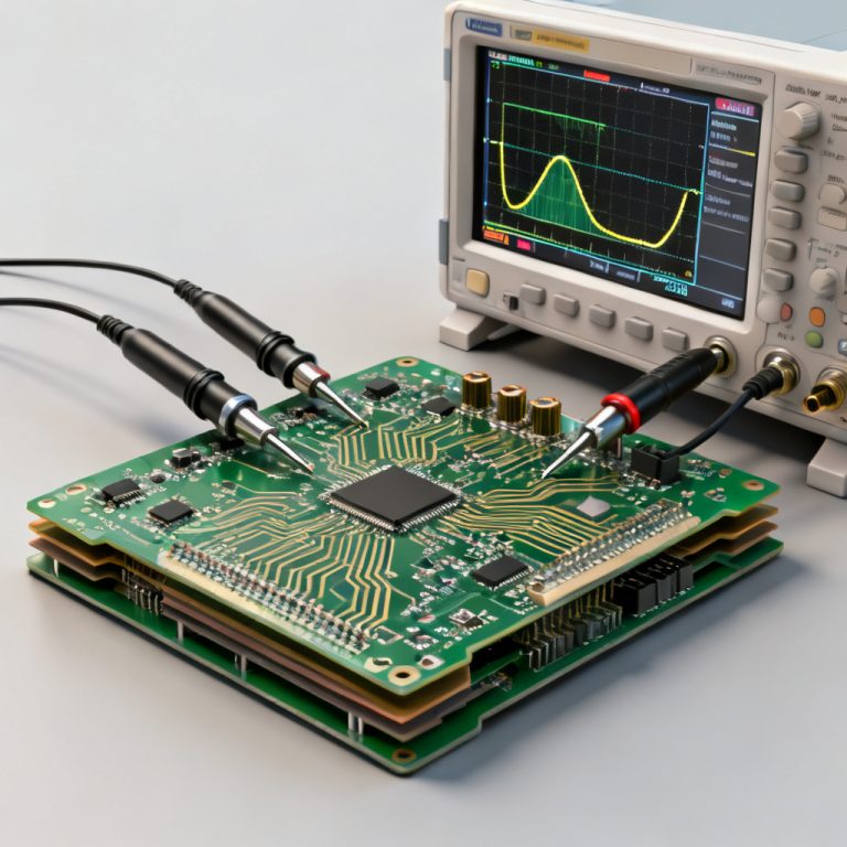
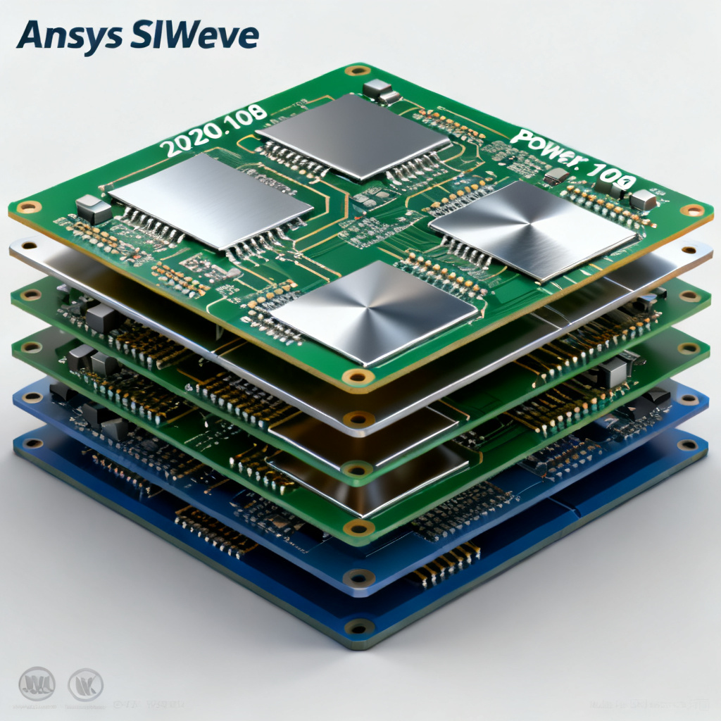
Setting up a Power Integrity PCB Simulation in Ansys SIwave is essential for high-speed PCB design, ensuring stable power delivery and signal integrity in B2B manufacturing. This guide integrates expert workflows from top-ranked sources to help you optimize your power distribution network (PDN) from pre-layout to validation.
1. Pre-Simulation Preparation for Power Integrity PCB Simulation
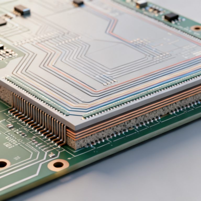
Initial Geometry and Material Setup
Begin your Power Integrity PCB Simulation by importing ODB++ or Gerber files into SIwave. Ensure the stackup includes all layers, vias, and power planes. Assign accurate dielectric constants (Dk) and loss tangents (Df) for each substrate—use frequency-dependent models like Djordjevic-Sarkar for high-speed designs. Identify all power and ground nets using the Net Manager to check for floating polygons.
DC Analysis Preparation
For DC IR-drop analysis in a Power Integrity PCB Simulation, simplify geometry by removing non-essential components. Define lumped ports at the VRM output and loads, assigning DC voltage (e.g., 1.8V) and current sinks (e.g., 2A). This step ensures accurate voltage drop predictions.
AC Analysis Pre-Check
Enable dielectric loss models in the Material Manager for AC analysis. Set the simulation frequency range from DC to 1 GHz with logarithmic steps to capture resonance peaks and impedance behavior critical for high-speed PCB performance.
2. DC IR-Drop Analysis in Power Integrity PCB Simulation
Setting Up the Simulation
Launch DC IR-Drop Analysis in your Power Integrity PCB Simulation. Use adaptive meshing with a maximum element size of 0.5 mm for power planes. Enable convergence criteria (e.g., 1 mV voltage tolerance) to balance accuracy and speed. Solve and monitor the convergence plot.
Interpreting Results
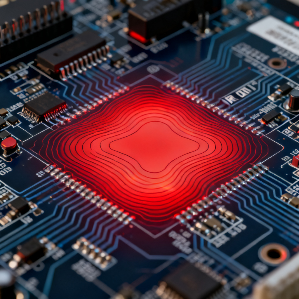
Examine the voltage contour map in your Power Integrity PCB Simulation. Ensure voltage at each load is within ±5% of target (e.g., 1.71V–1.89V for 1.8V rail). Check current density maps for hotspots—values exceeding 5 A/mm² require redesign. Use the resistance map to identify high-resistance paths, such as narrow traces causing 20 mV drop.
Optimization Workflow
Based on DC results, add decoupling capacitors near high-current loads. Use SIwave’s automatic placement for 0.1 µF and 1 µF caps. Re-run the DC analysis to verify voltage recovery and document final IR-drop values for manufacturing.
3. AC Impedance Analysis for Power Integrity PCB Simulation
Setting Up the AC Sweep
Create wave ports for AC analysis in your Power Integrity PCB Simulation. Place ports at VRM, load, and decap locations with 50-ohm impedance. Configure the sweep from 10 kHz to 1 GHz with 100 points per decade to capture low-frequency resonance and high-frequency bypass.
Running the Simulation
Launch AC Sweep Analysis and enable S-Parameter Output. Monitor residual error—if it exceeds 1e-6, refine the mesh near vias (e.g., 0.3 mm element size). This ensures accurate impedance profiles.
Interpreting the Z-Profile
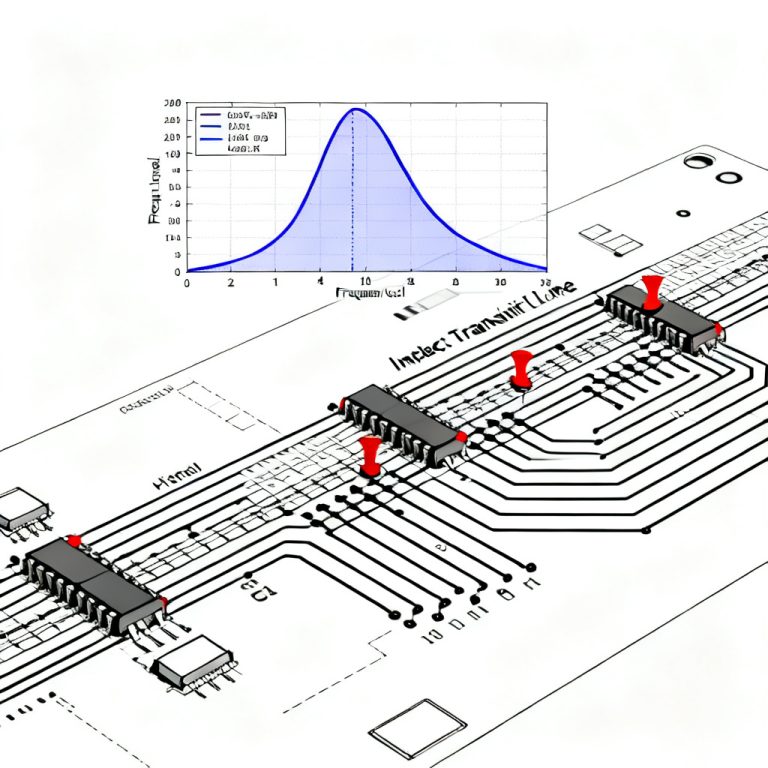
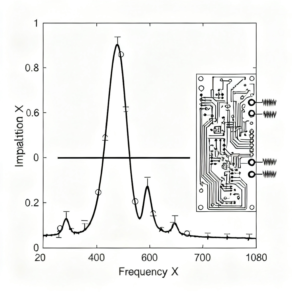
Plot Z11 (self-impedance) for the load port. Target impedance (Z_target) for high-speed ICs like FPGA or DDR is typically 10–100 mΩ up to 1 GHz. Identify resonance peaks above Z_target—for example, a 50 mΩ peak at 200 MHz indicates PDN resonance. Mitigate by adjusting decap values or adding ferrite beads. Examine Z12 for mutual coupling between power rails; if coupling exceeds -20 dB, add isolation slots or increase spacing.
4. Advanced Techniques in Power Integrity PCB Simulation
Via Modeling and 3D Effects
Use the Via Wizard to model via stubs in your Power Integrity PCB Simulation. For high-speed designs above 1 GHz, back-drill stubs to reduce resonance. Enable 3D Via Modeling for accurate parasitic extraction. Simulate plane pair resonance using the Eigenmode Solver to find resonant frequencies (e.g., 500 MHz for a 100 mm x 100 mm plane) and add decaps at antinodes.
Transient Analysis for Dynamic Loads
Set up time-domain simulation using a piecewise linear current source (e.g., 0–2A step at 1 ns rise time). Plot V(t) at the load—for DDR4, ripple should be below 50 mV peak-to-peak. Adjust decap ESR or add bulk capacitors if needed.
Thermal Coupling
Enable Joule Heating in DC IR-Drop Analysis to calculate temperature rise due to current density. For 1 oz copper, a 10°C rise is acceptable; higher values require thermal vias. Export power loss maps to Ansys Icepak for full thermal simulation, critical for high-power B2B boards (e.g., 100W+ servers).
5. Validation and Export for Power Integrity PCB Simulation
Cross-Check with Measurements
Compare simulated S-parameters with VNA data using SIwave’s validation tool. Ensure simulation matches measurement within 10% tolerance. Create a PI report including voltage maps, Z-profiles, and decap placement as a manufacturing spec.
Exporting for PCB Fabrication
Generate an IPC-2581 file with optimized layout, decap positions, and via patterns. Include manufacturing notes for back-drill depth and copper weight in the Gerber layer.
Final Checklist
Verify layer stackup adherence to assigned Dk/Df values. Run a final Design Rule Check in SIwave to flag violations, such as excessive via count near high-current paths.
FAQ: Power Integrity PCB Simulation in Ansys SIwave
What is the target impedance for a Power Integrity PCB Simulation?
In a Power Integrity PCB Simulation, target impedance for high-speed ICs like FPGA or DDR is typically 10–100 mΩ up to 1 GHz, ensuring stable power delivery.
How do I reduce resonance in AC analysis for Power Integrity PCB Simulation?
To reduce resonance in a Power Integrity PCB Simulation, adjust decoupling capacitor values, add ferrite beads, or modify plane shapes based on Z-profile peaks.
What tools are used for via modeling in Power Integrity PCB Simulation?
In a Power Integrity PCB Simulation, use SIwave’s Via Wizard for via stub modeling and 3D parasitic extraction, essential for high-speed designs above 1 GHz.
Why is thermal coupling important in Power Integrity PCB Simulation?
Thermal coupling in a Power Integrity PCB Simulation prevents overheating—enable Joule Heating to calculate temperature rise and ensure reliability for high-power B2B boards.
How do I validate a Power Integrity PCB Simulation with measurements?
Validate your Power Integrity PCB Simulation by comparing S-parameters with VNA data, aiming for within 10% tolerance to ensure manufacturing accuracy.
| Parameter | Specification for Power Integrity PCB Simulation | Typical Value |
|---|---|---|
| Target Impedance (Z_target) | Power Integrity PCB Simulation requirement | 10–100 mΩ up to 1 GHz |
| Voltage Tolerance | Power Integrity PCB Simulation IR-drop limit | ±5% of target voltage |
| Current Density Limit | Power Integrity PCB Simulation copper constraint | ≤5 A/mm² for 1 oz copper |
| Frequency Sweep Range | Power Integrity PCB Simulation AC analysis | 10 kHz to 1 GHz |
| Mesh Element Size | Power Integrity PCB Simulation DC analysis | 0.5 mm for power planes |
Power Integrity PCB Simulation in Ansys SIwave ensures high-speed PCB designs meet stringent performance requirements, reducing prototype iterations and guaranteeing first-pass success for B2B manufacturers. Contact our team for custom simulation services and high-speed PCB fabrication tailored to your design.