Performing DC drop simulation for power integrity PCB validation is essential for high-speed designs to prevent voltage failures. This guide covers the complete process from fundamentals to optimization.
Understanding DC Drop Simulation for Power Integrity PCB Validation
DC drop simulation for power integrity PCB validation relies on Ohm’s Law: V = I × R. In high-speed PCBs, resistance comes from copper planes, traces, vias, and connectors. High current draw from FPGAs or CPUs can cause voltage drops exceeding tolerance, leading to logic errors.
Key Metrics for DC Drop Analysis
| Metric | Definition | Impact on DC Drop Simulation for Power Integrity PCB Validation |
|---|---|---|
| Target Impedance | (Voltage × Tolerance) / Current | Maximum allowable PDN impedance |
| DC Resistance (DCR) | Total resistance from VRM to load | Directly determines voltage drop |
| Current Density | A/mm² in copper traces | High density causes heating and drop |
DC drop simulation for power integrity PCB validation must account for non-uniform current distribution in high-speed designs.
Data Preparation for DC Drop Simulation for Power Integrity PCB Validation
Accurate DC drop simulation for power integrity PCB validation requires precise input data.
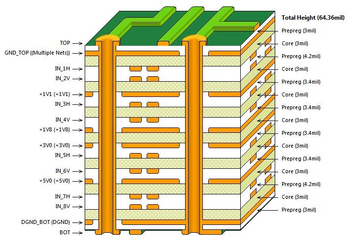
Stackup and Material Properties
Copper thickness (1 oz = 35 µm, 2 oz = 70 µm) and dielectric materials affect resistance. For high-speed PCBs, use solid power planes.
Component and Load Definitions
Define VRM output voltage, maximum current draw per IC, and voltage tolerance (e.g., ±3%). Include exact BGA pad locations.
Net and Shape Definitions
Export ODB++ or IPC-2581 from your layout tool. Include all copper pours, via arrays, and thermal reliefs.
Simulation Tools for DC Drop Simulation for Power Integrity PCB Validation
Three industry-standard tools for DC drop simulation for power integrity PCB validation are:
Ansys SIwave
Best for complex multi-layer designs. Offers 3D field solving, current density heatmaps, and automatic via resistance extraction.
Cadence Sigrity PowerDC
Ideal for enterprise designs. Features EM/thermal co-simulation and automated pass/fail reports.
Keysight PathWave ADS
Suited for RF/mixed-signal designs. Includes temperature-dependent resistivity and coupled AC/DC analysis.
Simulation Setup for DC Drop Simulation for Power Integrity PCB Validation
Configure these parameters for accurate DC drop simulation for power integrity PCB validation:
Material Resistivity and Temperature
Copper resistivity at 25°C: 1.72 × 10⁻⁸ Ω·m. Increase by 0.39% per °C for elevated temperatures.
Current Source and Sink Definitions
Place current source at VRM output. Distribute load current across all power pins of BGA devices.
Mesh and Solver Settings
Use fine mesh (0.1–0.5 mm) for high-current BGA fanout regions. Set convergence residual < 1e-6.
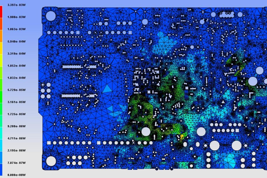
Interpreting Results from DC Drop Simulation for Power Integrity PCB Validation
DC drop simulation for power integrity PCB validation produces several outputs:
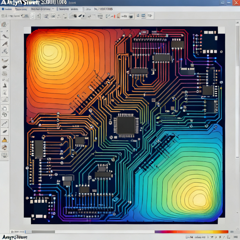
Voltage Contour Plot
Color gradient from red (high voltage near VRM) to blue (low voltage at load). Ensure all load pins exceed minimum tolerance (e.g., 0.97V for 1.0V rail).
Current Density Heatmap
Red zones indicate high current density. For 1 oz copper, keep below 10 A/mm²; for 2 oz, below 15 A/mm².
Voltage at Load Pins Report
Table showing each pin’s voltage. Aim for 10% margin above minimum.
Optimization Based on DC Drop Simulation for Power Integrity PCB Validation
If DC drop simulation for power integrity PCB validation shows violations, take these actions:
Increase Copper Thickness
Switch from 1 oz to 2 oz copper reduces resistance by 50%. Cost trade-off: thicker copper increases manufacturing difficulty.
Widen Traces and Use Solid Planes
Avoid neck-downs. Replace hatched planes with solid copper pours.
Add More Vias
Use multiple vias per power pin. Ten 0.3mm vias in parallel reduce resistance to 0.1–0.2 mΩ.
Optimize VRM Placement
Place regulator closer to high-current load. Use Kelvin sensing for feedback compensation.
Validation After DC Drop Simulation for Power Integrity PCB Validation
Post-manufacturing, verify with four-point Kelvin measurement and thermal imaging. Compare measured drop with simulation; adjust model if deviation exceeds 10%.