Power Integrity PCB Modeling is essential for designing reliable high-speed PCBs. This guide covers creating accurate VRM and load models for PDN simulation, ensuring stable voltage delivery and minimal noise in your high-speed PCB designs.

Understanding the Power Distribution Network for Power Integrity PCB Modeling
What is a PDN in High-Speed PCB Design?
The Power Distribution Network (PDN) delivers stable voltage from the VRM to all active devices on the PCB. In Power Integrity PCB Modeling, the PDN includes the VRM, decoupling capacitors, PCB power planes, vias, and interconnects. The goal is to maintain impedance below a target value across a wide frequency range.
Why Power Integrity PCB Modeling Matters for High-Speed Applications
The PDN behaves differently at low frequencies (DC) and high frequencies (GHz). Capacitors have parasitic inductance (ESL) and resistance (ESR), planes act as resonant cavities, and vias introduce inductive discontinuities. Without accurate Power Integrity PCB Modeling, simulations fail to predict real-world noise, leading to costly redesigns. In high-speed PCBs, the PDN must supply fast transient currents, making precise VRM and load models critical.
Creating Accurate VRM Models for Power Integrity PCB Modeling
The VRM is the source of the PDN. Its model must capture DC regulation, output impedance, and transient response for effective Power Integrity PCB Modeling.
Types of VRM Models in Power Integrity PCB Modeling
Ideal Voltage Source: Simple but unrealistic for high-frequency analysis. Use only for initial DC checks. Average Model: Uses a voltage source with series resistance (R_out) and inductance (L_out). Suitable for frequencies up to 1 MHz. Switching Model: Includes PWM controller, MOSFETs, inductor, and output capacitor. Accurate for transient analysis but computationally heavy. Frequency-Dependent Impedance Model: Uses S-parameters or a 2-port network to represent VRM output impedance (Z_out). Ideal for PI analysis up to 1 GHz.
Key Parameters for VRM Modeling in High-Speed PCB
DC Output Voltage: Set to the nominal value. Output Impedance (Z_out): Typically 1-10 mΩ at DC, rising to 100 mΩ at high frequencies due to inductor and capacitor parasitics. Loop Bandwidth: The VRM control loop gain bandwidth determines transient response. Ripple and Noise: Include switching frequency and output ripple amplitude.
Step-by-Step VRM Model Creation for Power Integrity PCB Modeling
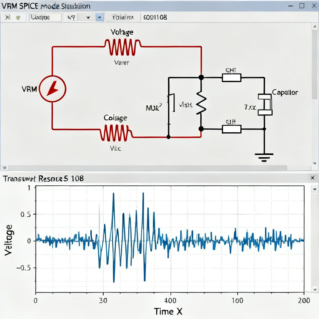
Step 1: Extract Datasheet Parameters. From the VRM IC datasheet, note output voltage accuracy, load regulation, transient response time, and output capacitance. Step 2: Build a Behavioral SPICE Model. Use a voltage source with value = V_out, add series resistance R_out = V_drop / I_max, and series inductance L_out = (R_out * τ) / 2. Include output capacitor C_out with ESR and ESL from datasheet. Step 3: Create a Frequency-Dependent Impedance Model. Use a 2-port S-parameter block in simulation tools. Measure Z_out using a VNA from 1 kHz to 1 GHz. Fit to a rational function using Vector Fitting. Step 4: Validate with Transient Simulation. Apply a 1A step load and observe voltage droop. Adjust R_out and L_out until droop matches datasheet.
Common VRM Modeling Mistakes in Power Integrity PCB Modeling
Ignoring ESL of Output Capacitors leads to overly optimistic high-frequency impedance. Using Ideal Voltage Source misses transient droop and loop response. Neglecting PCB Parasitics adds inductance from VRM output traces and vias, shifting resonance peaks.
Creating Accurate Load Models for Power Integrity PCB Modeling
The load draws current from the PDN. Its model must capture transient current demands, on-die capacitance, and package parasitics for accurate Power Integrity PCB Modeling.
Types of Load Models in Power Integrity PCB Modeling
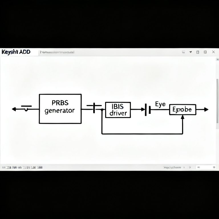
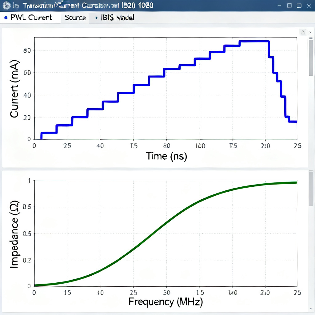
Constant Current Source: Simple but ignores transient behavior. Time-Dependent Current Source (PWL): Uses a piecewise linear current waveform. IBIS Model: Includes I/O driver current profiles and package RLC. On-Die Capacitance Model: Represents the die’s decoupling capacitance. S-Parameter Load Model: Measures load impedance using a VNA.
Key Parameters for Load Modeling in High-Speed PCB
Peak Current (I_peak): Maximum current draw during switching. Slew Rate (di/dt): Rate of current change determines voltage droop via L*di/dt. On-Die Capacitance (C_die): Provides local charge storage. Package Inductance (L_pkg): Bond wires and solder balls add 1-10 nH. Operating Frequency: Clock speed determines transient current harmonics.
Step-by-Step Load Model Creation for Power Integrity PCB Modeling
Step 1: Gather Load Data. From the load IC datasheet or IBIS file, note I_peak, I_avg, switching frequency, package type, and on-die capacitance. Step 2: Create a PWL Current Source. In SPICE, define a current source with a piecewise linear waveform. Add a series resistor R_load = V_out / I_avg to represent DC load. Step 3: Model the Package Parasitics. Add a series inductor L_pkg and resistor R_pkg between the current source and PCB connection. Include a shunt capacitor C_die with ESR and ESL in parallel. Step 4: Create an IBIS-Based Model. Use an IBIS model from the IC vendor. Extract the Power Clamp and GND Clamp tables for I/O buffer current. Step 5: Validate with Impedance Profile. Simulate Z_load from 1 MHz to 10 GHz. The profile should show a low-impedance region, a resonance peak, and rising impedance. Adjust C_die and L_pkg to match measured data.
Common Load Modeling Mistakes in Power Integrity PCB Modeling
Using a Simple Capacitor Only misses transient current dynamics. Ignoring Package Inductance leads to overestimated high-frequency performance. Assuming Constant Current misses high-frequency current harmonics that excite PDN resonances.
Integrating VRM and Load Models for PDN Simulation
Building the Complete PDN Model for Power Integrity PCB Modeling
Components: VRM model + PCB power planes (modeled as RLC or S-parameters) + decoupling capacitors (with ESR/ESL) + vias (with inductance) + load model. Topology: Connect VRM output to PCB planes, then to decoupling caps, then to load.
Simulation Types for Power Integrity PCB Modeling
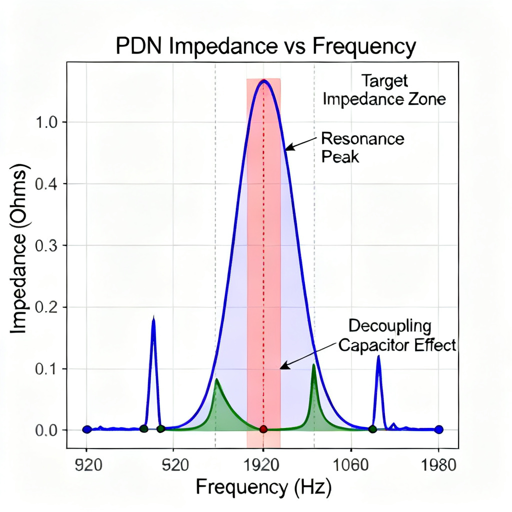
DC Analysis: Check voltage drop across the PDN. Transient Analysis: Apply a step load and observe voltage at the load. AC Impedance Analysis: Sweep frequency from 1 kHz to 10 GHz. Target Z_PDN below target impedance across all frequencies.
Case Study: High-Speed FPGA PDN with Power Integrity PCB Modeling
VRM: 1.2V, 10A, behavioral model with R_out=10 mΩ, L_out=250 nH, C_out=100 µF. PCB: 4-layer stackup, power plane 0.5 oz copper. Decoupling Caps: 10x 100 nF, 4x 10 µF. Load: FPGA with I_peak=8A, di/dt=1A/ns, C_die=50 nF, L_pkg=2 nH. Simulation Result: Z_PDN peaks at 0.15Ω at 1.2 GHz. Add 4x 1 µF caps to damp resonance. Final Z_PDN below 0.1Ω up to 5 GHz.
Tools for Power Integrity PCB Modeling
Ansys SIwave: Full-wave 3D EM solver for PDN impedance and transient analysis. Cadence Sigrity: Specialized for PI and SI co-simulation. Keysight ADS: Circuit-based simulation with S-parameter blocks. Open-Source Options: Qucs but limited for high-frequency.
Advanced Techniques and Best Practices for Power Integrity PCB Modeling
Using S-Parameters for VRM and Load Models
S-parameters capture phase and magnitude of impedance up to 40 GHz. Measure VRM output and load input with a VNA. De-embed fixture effects. Use Touchstone files in simulation. Requires measurement equipment and careful calibration.
Including Temperature Effects in Power Integrity PCB Modeling
ESR of capacitors increases with temperature. VRM output impedance shifts due to thermal drift. Use temperature-dependent SPICE models or derate ESR by 50% for worst-case analysis.
Correlation with Measurements for Power Integrity PCB Modeling
Build a test PCB with VRM and load. Measure PDN impedance with a VNA. Compare to simulation. Adjust capacitor ESL/ESR and plane inductance until correlation within 10%. Common discrepancies include via inductance underestimated and plane resonance shifted due to dielectric constant tolerance.
Best Practices for High-Speed PCB Design Using Power Integrity PCB Modeling
Minimize Loop Inductance: Place decoupling caps as close to load pins as possible. Use Multiple Via Connections: 2-4 vias per cap reduce inductance by 50%. Optimize Power Plane Shape: Avoid slots and splits. Model Up to 5th Harmonic: For a 1 GHz clock, simulate up to 5 GHz to capture all PDN resonances.
Conclusion: Achieving Reliable Power Integrity with Accurate Modeling
Accurate VRM and load models are the cornerstone of Power Integrity PCB Modeling in high-speed PCB design. By combining behavioral SPICE models for low frequencies, IBIS and PWL sources for transient analysis, and S-parameters for high frequencies, you can predict and mitigate PDN issues before fabrication. For your High-Speed PCB manufacturing business, offering PI modeling services adds significant value to clients designing advanced FPGAs, ASICs, and memory interfaces.
Frequently Asked Questions About Power Integrity PCB Modeling
What is Power Integrity PCB Modeling?
Power Integrity PCB Modeling is the process of creating accurate VRM and load models to simulate the Power Distribution Network (PDN) behavior in high-speed PCBs.
Why are accurate VRM models important for Power Integrity PCB Modeling?
Accurate VRM models capture DC regulation, output impedance, and transient response, which are critical for predicting voltage droop and noise in high-speed PCB designs.
How do I create a load model for Power Integrity PCB Modeling?
Create a load model by gathering datasheet parameters, building a PWL current source, modeling package parasitics, and validating with an impedance profile.
What tools are used for Power Integrity PCB Modeling?
Common tools include Ansys SIwave, Cadence Sigrity, and Keysight ADS for simulating PDN impedance and transient behavior.
What are common mistakes in Power Integrity PCB Modeling?
Common mistakes include ignoring ESL of output capacitors, using ideal voltage sources, and neglecting package inductance in load models.
| Parameter | VRM Model Value | Load Model Value |
|---|---|---|
| Output Voltage | 1.2V | N/A |
| Output Impedance | 10 mΩ at DC | N/A |
| Peak Current | 10A | 8A |
| Slew Rate | N/A | 1A/ns |
| On-Die Capacitance | N/A | 50 nF |
| Package Inductance | N/A | 2 nH |