Power Integrity PCB Resonance detection via Frequency Domain Analysis is the definitive method for ensuring high-speed PCB reliability. This guide synthesizes the most authoritative industry practices to help you identify and mitigate resonant impedance peaks in your Power Distribution Network (PDN).
What Is Power Integrity PCB Resonance and Why Does It Matter?
Power Integrity PCB Resonance occurs when the PDN—composed of power and ground planes, vias, and decoupling capacitors—exhibits high impedance at specific frequencies. This is not a simple DC resistance issue; it is an AC impedance problem driven by the distributed inductance and capacitance of the board.
Physical Mechanism of PCB Resonance
Parallel plate resonance emerges when power and ground planes form a natural capacitor, but finite dielectric thickness and board dimensions create a cavity. When the electrical length equals a quarter or half wavelength of a signal frequency, standing waves form, causing impedance peaks that can spike 10x to 100x higher than the target impedance.
Consequences of Unchecked Resonance
Voltage droop occurs when core voltage collapses during high-speed IC switching. Simultaneous Switching Noise (SSN) couples noise between ICs through the resonant PDN, and radiated emissions cause EMC failures as resonant cavities act as unintentional antennas.
Why Frequency Domain Analysis Is Essential
Time-domain analysis shows the effect of resonance, but Frequency Domain Analysis reveals the root cause. By plotting impedance vs. frequency, you directly identify resonant peaks and their Q-factors for robust PDN design.
Core Methodology: Frequency Domain Analysis for Power Integrity PCB Resonance
The foundation of any Frequency Domain Analysis for Power Integrity PCB Resonance is the target impedance (Z_target). This is the maximum allowable impedance of the PDN at any frequency, calculated as Z_target = (Vdd * Ripple%) / I_transient. For a 1.0V supply with 3% ripple and a 5A transient, Z_target equals 6 mΩ.

Step 1: Define Target Impedance and Frequency Range
Frequency Domain Analysis for Power Integrity PCB Resonance must cover from DC up to the maximum harmonic of your fastest signal, typically 10x the clock frequency. For a 10 Gbps signal, the 5th harmonic is 25 GHz; your simulation should extend to at least 20–40 GHz.
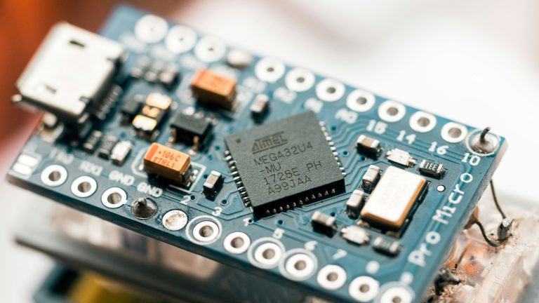
Step 2: Build the PDN Model
Two primary modeling approaches exist: lumped element models (SPICE) for frequencies below 1 GHz, and full-wave electromagnetic simulation (S-parameters) as the gold standard for high-speed boards. Tools like Ansys SIwave, Keysight ADS, or Cadence Sigrity extract multi-port S-parameter models that inherently include plane cavity resonance, via anti-pad effects, and mutual coupling between capacitors.
Step 3: Simulate the Impedance Profile
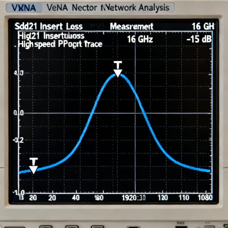
Set up a port at the IC’s power pin and sweep frequency from 1 MHz to the upper limit. Extract Z11 and plot it on a log-log scale. Look for sharp peaks where impedance exceeds Z_target; these indicate resonance frequencies and high Q-factors that amplify noise.
Step 4: Identify and Interpret Resonant Peaks
On the Z11 plot, anti-resonance peaks often occur where inductive impedance of the plane and capacitive impedance of a decoupling capacitor cancel out. This is the most common cause of PDN failure. A high Q (narrow, tall peak) indicates dangerous underdamped resonance.
Advanced Detection Techniques for Power Integrity PCB Resonance
Beyond Z11, three advanced techniques provide deeper insight into Power Integrity PCB Resonance behavior.
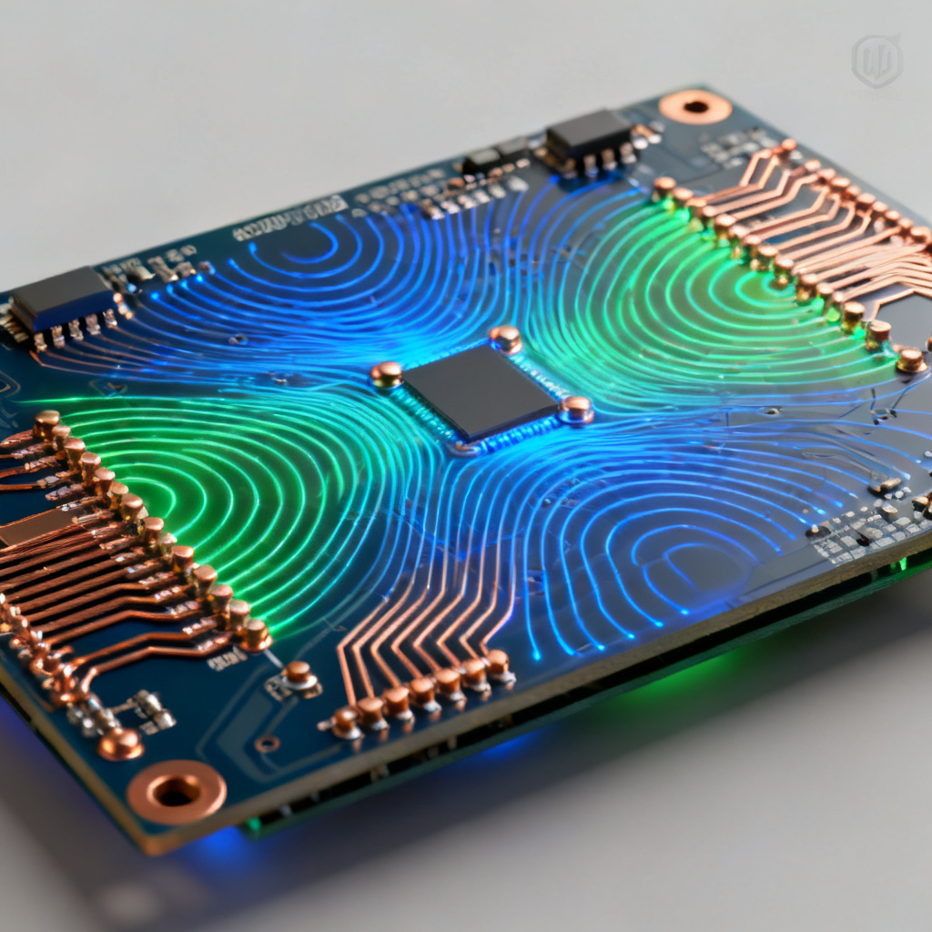
Voltage Distribution Maps
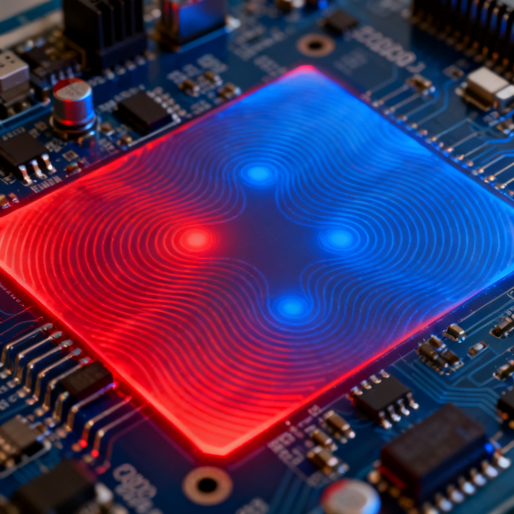
Simulate voltage distribution across the entire power plane at the resonant frequency. Standing wave patterns reveal hotspots and nulls. Place high-current ICs away from resonant hotspots to ensure uniform power delivery.
Transfer Impedance (Z21)
Z21 measures impedance between aggressor and victim ICs. High Z21 at a specific frequency means noise directly couples through the PDN. Use ferrite beads, split planes, or component relocation to mitigate crosstalk.
Loop Inductance Analysis
From the Z11 plot, the inductive region (slope of +20 dB/decade) reveals loop inductance: L_loop = Z_inductive / (2πf). High loop inductance lowers resonant frequency and increases peak impedance. Minimize loop inductance by placing decoupling capacitors close to the IC and using thin dielectrics between power and ground.
Practical Mitigation Strategies Based on Frequency Domain Analysis
Let the data from Frequency Domain Analysis for Power Integrity PCB Resonance guide your mitigation efforts.
Optimize Decoupling Capacitor Selection and Placement
Target the resonance frequency directly. For a 50 MHz resonance, use a 100 nF capacitor; for 500 MHz, use 10 nF or 1 nF. Use capacitor spreading (e.g., 10 µF, 1 µF, 100 nF, 10 nF) and simulate combined impedance to avoid anti-resonance peaks. Place capacitors directly under power pins with multiple vias in parallel to reduce loop inductance.
Adjust Plane Geometry
Reduce cavity size by using power islands or moats to break large planes into smaller, non-resonant sections. Increase dielectric thickness to lower resonant frequency, but balance with loop inductance. Use embedded capacitance with thin, high-Dk dielectric layers (e.g., 2 mils, Dk=10) to shift resonances to higher, less problematic frequencies.
Use Damping and Via Stitching
Add resistive damping with small resistors (0.1–1 Ω) in series with bulk capacitors to reduce Q. For GHz-range resonance, consider lossy dielectrics like Rogers 4350B or resistive material layers. Place stitching ground vias within 100 mils of every signal via transitioning through power planes to reduce return path inductance and suppress plane resonances.
Common Pitfalls in Power Integrity PCB Resonance Analysis
Avoid these frequent mistakes when performing Frequency Domain Analysis for Power Integrity PCB Resonance.
| Pitfall | Impact | Solution |
|---|---|---|
| Ignoring DC Drop | Voltage at IC out of tolerance | Run separate DC simulation |
| Using Ideal Capacitor Models | Inaccurate impedance peaks | Use vendor S-parameter models |
| Simulating Without Package | Missing package inductance effects | Include package model |
| Focusing Only on Z11 | Ignoring noise coupling (Z21) | Analyze transfer impedance |
| Over-Designing Capacitors | Creates anti-resonance peaks | Use targeted, simulated approach |
FAQ: Power Integrity PCB Resonance and Frequency Domain Analysis
What is the target impedance for Power Integrity PCB Resonance?
The target impedance for Power Integrity PCB Resonance is calculated as Z_target = (Vdd * Ripple%) / I_transient, typically below 10 mΩ for modern high-speed designs.
How does Frequency Domain Analysis detect PCB resonance?
Frequency Domain Analysis for Power Integrity PCB Resonance measures Z11 impedance across frequency, revealing sharp peaks where resonance occurs, enabling targeted mitigation.
What causes anti-resonance in a PDN?
Anti-resonance in Power Integrity PCB Resonance arises when inductive plane impedance cancels capacitive decoupling impedance at a specific frequency, creating a high-impedance peak.
Why is loop inductance critical for Power Integrity PCB Resonance?
Loop inductance directly affects resonant frequency and peak impedance. Lower loop inductance shifts resonance higher and reduces peak amplitude, improving power integrity.
What is the best tool for Frequency Domain Analysis?
Full-wave EM solvers like Ansys SIwave, Keysight ADS, or Cadence Sigrity are industry standards for accurate Power Integrity PCB Resonance detection.
Conclusion: From Analysis to First-Pass Success
Frequency Domain Analysis for Power Integrity PCB Resonance transforms PDN design from guesswork to precision engineering. By simulating first, identifying peaks, mitigating with targeted strategies, and validating with time-domain transient simulation, you ensure your high-speed PCB meets performance targets.
At Your Company Name, we specialize in manufacturing high-speed PCBs with optimized power integrity. Our engineering team uses advanced Frequency Domain Analysis to ensure resonance-free designs. Contact us today for a free PDN review and quote on your next prototype or production run.