Understanding how to set up and interpret Power Integrity PCB results in Cadence Sigrity is essential for designing reliable high-speed PCBs in B2B export applications. This guide provides a complete, step-by-step methodology for DC, AC, and transient simulation, ensuring stable voltage delivery to FPGAs, ASICs, and high-speed ADCs.
Power Integrity Fundamentals in Sigrity
Before diving into setup, grasp the core principles that Sigrity addresses. Power Integrity PCB focuses on maintaining stable voltage supply within tight tolerances (typically ±3% to ±5% of nominal voltage) across the entire frequency range. Key challenges include DC voltage drop (IR drop), AC impedance, transient response, and resonance. Sigrity’s tools—PowerDC, PowerSI, and SpeedXP—are designed to address these systematically.

Key PDN Challenges
- DC Voltage Drop (IR Drop): Caused by resistance in traces, planes, and vias.
- AC Impedance: Must remain low across frequency to minimize ripple.
- Transient Response: Quick response to di/dt events without droop or overshoot.
- Resonance: Capacitor/plane interaction can create noise peaks.
Pre-Layout Setup: Defining the PDN Model
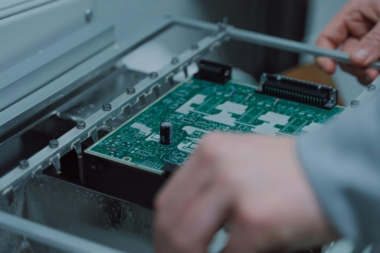
A successful Power Integrity PCB analysis begins before layout. The pre-layout phase in Sigrity involves creating a virtual PDN model to validate component selection and decoupling strategies.
Importing the Design
Import the PCB layout file (ODB++, IPC-2581, or Allegro .brd) into Sigrity. Ensure all layers, vias, and component footprints are correctly mapped. For pre-layout studies, create a simplified stackup using Sigrity System Explorer.
Defining the Power Delivery Network
Identify all power nets (e.g., VDD_CORE, VDD_IO, AVDD) and ground nets. Assign voltage sources at the VRM location, specify current sinks at IC pins with datasheet profiles, and include decoupling capacitors with ESR/ESL values.
Setting Up the Stackup
In PowerDC or PowerSI, define copper thickness (e.g., 1 oz, 2 oz), dielectric material (e.g., FR4, Megtron 6, Rogers), plane layers, and via geometry. Accurate stackup parameters are critical for plane capacitance and inductance.
Decoupling Capacitor Selection
Using Sigrity’s Decoupling Capacitor Optimizer, target a specific impedance profile (e.g., < 0.1Ω up to 1 GHz). Place capacitors close to the load, mix low-ESR ceramic for high frequencies and bulk for low frequencies, and simulate mounting inductance effects.

DC Power Integrity Analysis Using PowerDC
DC analysis is the first step in evaluating the PDN’s ability to deliver steady-state voltage. It is performed using Sigrity PowerDC.
Setting Up the DC Simulation
Open the design in PowerDC, assign voltage sources with nominal output (e.g., 1.2V), assign current sinks to IC pins (e.g., 5A for core rail), define simulation boundary, and set convergence criteria.
Running the Simulation
Click Simulate to compute voltage distribution, current density, and power dissipation due to resistive losses (I²R).
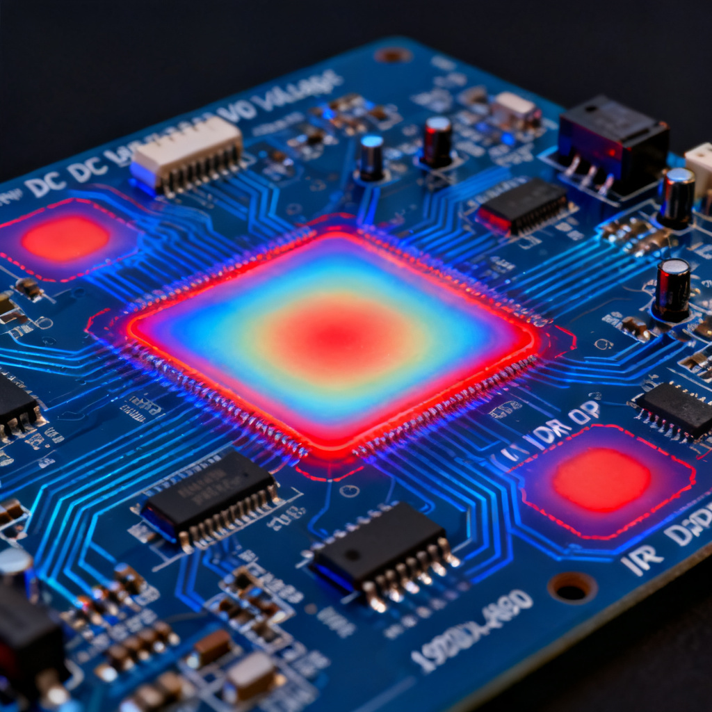
Interpreting DC Results
| Parameter | Target | Action if Exceeded |
|---|---|---|
| IR Drop | < 50-70 mV for 1.2V rail | Add copper pours, wider traces, more vias |
| Current Density | < 30 A/mm² for 1 oz copper | Wider traces, thicker copper, additional vias |
| Power Loss | < 1W per region | Optimize routing, reduce resistance |
Actionable Insights: If IR drop is too high, add copper pours, increase trace width, use more vias, or move VRM closer to load. If current density is high, use multiple parallel vias (e.g., 4-6 vias per amp) and ensure via stitching.
AC Impedance Analysis Using PowerSI
AC impedance analysis (PDN impedance profiling) is performed using Sigrity PowerSI to ensure low impedance across the frequency range (e.g., DC to 10 GHz for high-speed digital).
Setting Up the AC Simulation
Define simulation type as AC Sweep, set frequency range from 10 Hz to 10 GHz, specify 1000 logarithmically spaced points, and assign ports at VRM output and IC power pins.
Including Parasitics
Enable via modeling for parasitic inductance/capacitance, include plane pair resonance via stackup properties, and add decoupling capacitor models with ESL/ESR (use vendor S-parameters if available).
Running the Simulation
Click Simulate to compute impedance vs. frequency and S-parameters (S11, S21) for the PDN.
Interpreting AC Impedance Results
Target Impedance: Z_target = (V_nominal × tolerance) / I_max. For 1.2V ±5% and 10A peak, Z_target = 60 mV/10A = 6 mΩ. Look for resonant peaks above Z_target, indicating anti-resonance between capacitors and plane capacitance. A flat impedance profile (within ±20% of Z_target) is ideal.
Actionable Insights: For peaks at low frequencies (1-10 MHz), add bulk capacitors (10-100 µF) with low ESR. For mid-frequencies (10-100 MHz), adjust capacitor values to create valleys. For high frequencies (>1 GHz), reduce via inductance with shorter vias, larger antipads, or ground stitching vias.
Transient Simulation Using SpeedXP
Transient analysis (time-domain ripple) is performed using Sigrity SpeedXP to evaluate PDN response to dynamic current loads like clock gating or data bus switching.
Setting Up the Transient Simulation
Import PDN model from PowerSI (including S-parameters and capacitor models). Define a current profile (PWL waveform) for the load (e.g., step from 0A to 5A in 1 ns). Set simulation time (e.g., 0 to 10 µs) and time step (e.g., 10 ps).
Running the Simulation
Click Simulate to compute voltage waveform at the load, showing droop, overshoot, and ripple.
Interpreting Transient Results
Droop Magnitude: Should be within tolerance (e.g., < 60 mV for 1.2V rail). Settling Time: Stabilize within 1% of nominal within a few clock cycles (e.g., < 10 ns for 1 GHz clock). Ripple Amplitude: High-frequency ripple >10 mV peak-to-peak indicates inadequate high-frequency decoupling.
Actionable Insights: If droop is too large, add bulk capacitance or reduce VRM-to-load distance. If ripple is too high, use smaller-value, low-ESL capacitors (e.g., 0.1 µF, 0.01 µF) closer to IC pins. If settling time is long, improve damping by increasing ESR in some capacitors.
Advanced Interpretation and Optimization
Combining DC and AC Results
A robust PDN must satisfy both DC and AC requirements. Use Sigrity PDN Analyzer to ensure DC voltage stays within tolerance, AC impedance stays below Z_target, and transient excursions are within limits.
Resonance Mitigation Strategies
Use a spread of capacitor values (e.g., 10 µF, 1 µF, 0.1 µF, 0.01 µF) to create overlapping impedance valleys. Increase plane capacitance with thinner prepreg or embedded capacitance layers. Reduce via inductance with larger diameters, shorter stubs (back-drilling), and ground vias adjacent to signal vias.
Correlation with Measurements
Validate simulation results with VNA for AC impedance, oscilloscope for transient voltage, and DC multimeter for IR drop. Sigrity’s Correlation Workbench helps align simulation with measured data by adjusting material properties and parasitics.
Common Pitfalls and Best Practices
Pitfalls to Avoid
- Ignoring via inductance—vias are the largest source of high-frequency impedance.
- Using ideal capacitor models—always use vendor S-parameter models with ESL/ESR.
- Neglecting plane resonance—simulate full stackup to avoid unexpected peaks.
- Overlooking thermal effects—use PowerDC with thermal coupling for high current density.
Best Practices for B2B Export PCB Design
- Design for margin: target PDN impedance 50% lower than calculated Z_target.
- Use simulation-driven decoupling to minimize capacitor count while meeting requirements.
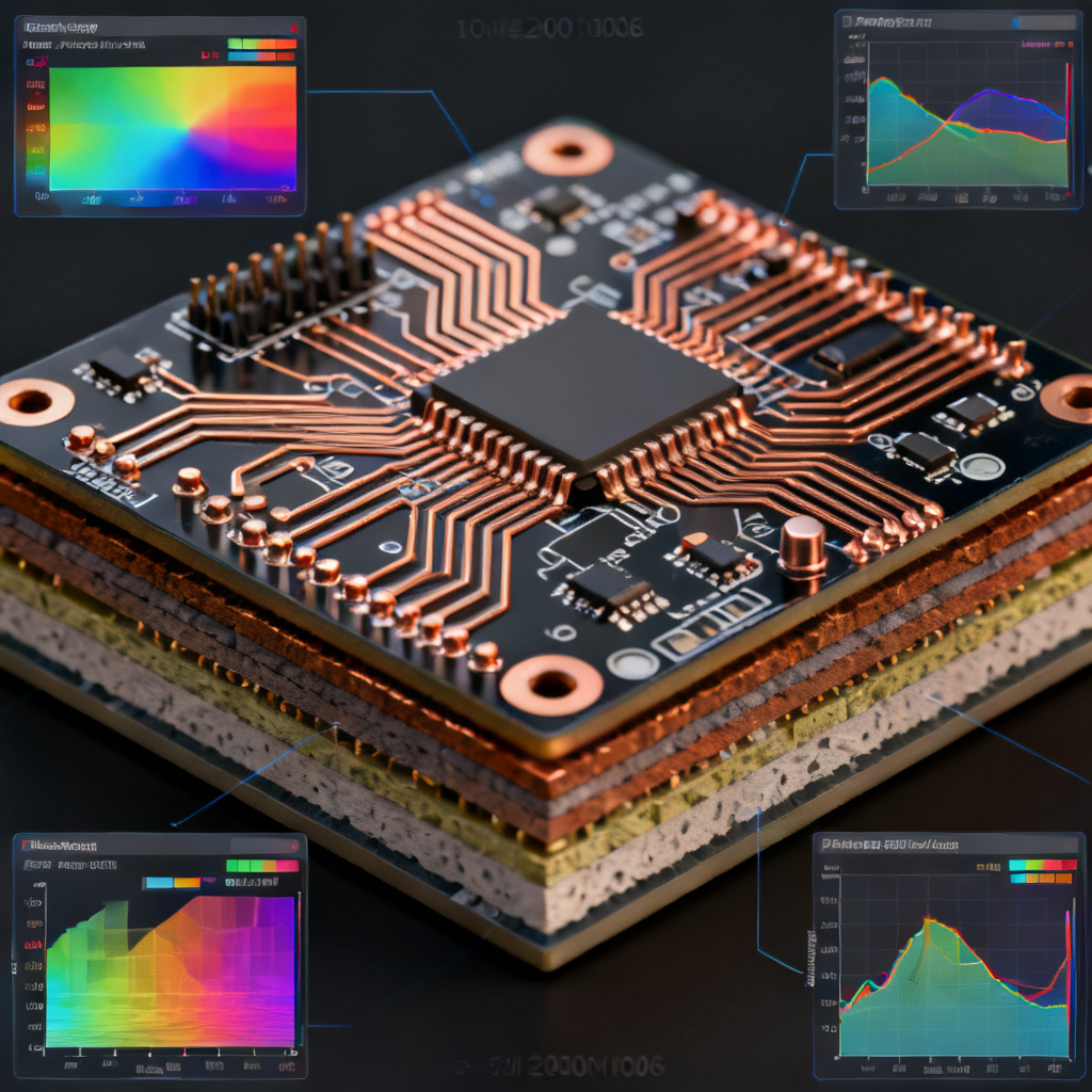
- Document results (voltage contours, impedance plots, transient waveforms) for customer validation.
- Iterate early with pre-layout PI analysis to avoid costly redesigns.
FAQ: Power Integrity PCB in Cadence Sigrity
What is Power Integrity PCB analysis in Cadence Sigrity?
Power Integrity PCB analysis in Cadence Sigrity involves simulating the power distribution network (PDN) to ensure stable voltage delivery, using tools like PowerDC for DC analysis, PowerSI for AC impedance, and SpeedXP for transient simulation.
How do I set up a Power Integrity PCB simulation in Sigrity?
To set up a Power Integrity PCB simulation, import your layout, define the PDN with VRM and current sinks, configure the stackup, and run DC, AC, or transient simulations in PowerDC, PowerSI, or SpeedXP respectively.
What is target impedance in Power Integrity PCB design?
Target impedance is calculated as Z_target = (V_nominal × tolerance) / I_max. For Power Integrity PCB, keeping impedance below this value across all frequencies ensures minimal voltage ripple and stable operation.
How do I interpret IR drop results in PowerDC?
In Power Integrity PCB analysis, IR drop results show voltage distribution. If the drop exceeds 50-70 mV (for a 1.2V rail), the PDN has excessive resistance—add copper pours, wider traces, or more vias to reduce it.
What causes resonant peaks in Power Integrity PCB impedance plots?
Resonant peaks in Power Integrity PCB impedance plots are caused by anti-resonance between decoupling capacitors and plane capacitance. Mitigate by using a spread of capacitor values and optimizing via inductance.