[rank_math_breadcrumb]
In high-speed PCB design, differential pair impedance for microstrip vs stripline requires different formulas, as the electromagnetic fields and reference planes differ fundamentally. This page provides complete, authoritative guidance for achieving 100Ω or 90Ω target impedance in both topologies, helping you avoid costly signal integrity errors.
Whether you are routing USB, HDMI, PCIe, or Gigabit Ethernet, the impedance of your differential pair must match the system’s target—typically 100Ω or 90Ω. However, a common and costly misconception is that the same formula or design approach applies to both microstrip (outer layer) and stripline (inner layer) structures. This is fundamentally incorrect. The electromagnetic fields, reference planes, and manufacturing tolerances differ significantly between the two. As a result, the formulas for calculating differential pair impedance are distinct, and the design trade-offs are unique to each topology. This pillar page provides a complete, authoritative guide to understanding, calculating, and optimizing differential pair impedance for both microstrip and stripline configurations.
1. Understanding the Fundamentals: Microstrip vs Stripline
Before diving into formulas, it is critical to understand the physical differences between these two transmission line structures.
Microstrip (Outer Layer)
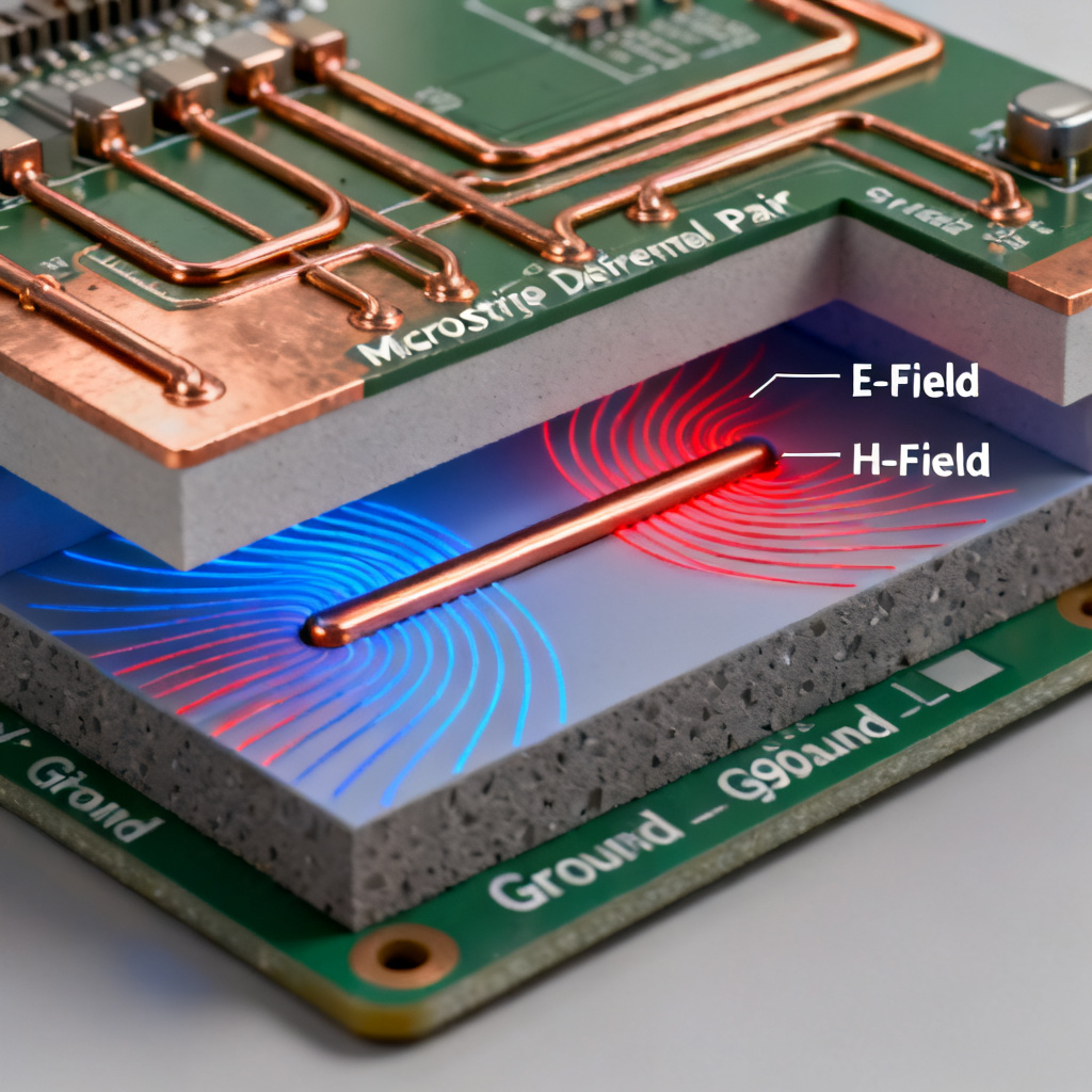
A microstrip line consists of a conductor (trace) on an outer layer of the PCB, separated by a dielectric material from a single reference plane (usually a ground or power plane). The top of the trace is exposed to air or solder mask.
Key Characteristics of Microstrip:
- Exposed Field: The electric and magnetic fields are partially in the air (εr ≈ 1) and partially in the dielectric (FR-4 εr ≈ 4.2-4.5). This creates an effective dielectric constant (εr_eff) that is lower than the bulk dielectric constant.
- Faster Propagation: Signals travel faster on microstrip layers due to the lower effective dielectric constant.
- More Radiated EMI: The exposed fields make microstrip lines more susceptible to crosstalk and electromagnetic interference (EMI).
- Easier Access: Components and test points are easily accessible on outer layers.
Stripline (Inner Layer)
A stripline is a conductor sandwiched between two reference planes, fully embedded in a homogeneous dielectric material. There are two common types: symmetric stripline (trace centered between two planes) and offset stripline (trace closer to one plane).
Key Characteristics of Stripline:
- Homogeneous Field: The fields are entirely contained within the dielectric material. The effective dielectric constant is essentially equal to the bulk dielectric constant (εr).
- Slower Propagation: Signals travel slower than on microstrip because the field is fully in the dielectric.
- Superior Shielding: The two reference planes provide excellent isolation from external noise and reduce EMI radiation.
- More Complex Fabrication: Inner layers are harder to probe and require more precise lamination control.
2. The Core Formulas: Why They Are Different
The most trusted industry references—including the IPC-2141A standard, Polar Instruments’ Si9000 field solver, and Altium Designer’s built-in impedance calculator—all converge on the same conclusion: you cannot use a single formula for both topologies. Here are the precise formulas and the reasoning behind them.
Differential Pair Impedance for Edge-Coupled Microstrip
For a differential pair on an outer layer, the formula is derived from the single-ended impedance (Z₀) and the coupling coefficient.
The Standard Microstrip Formula (approximate, for edge-coupled pairs):
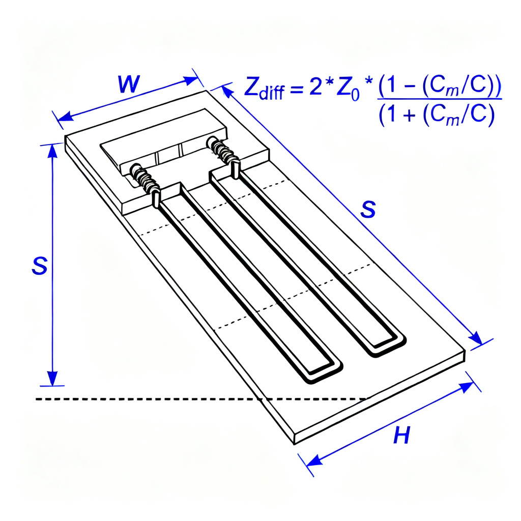
Zdiff_micro ≈ 2 × Z0_micro × (1 – 0.48 × e-0.96 × S/H)
Where:
- Z0_micro = Single-ended characteristic impedance of a microstrip line.
- S = Edge-to-edge spacing between the two traces.
- H = Dielectric height from the trace to the reference plane.
Why this formula is unique for microstrip: The exponential term accounts for the fringing fields that extend into the air. As the spacing (S) decreases relative to height (H), the coupling increases, and the differential pair impedance drops. The factor 0.48 and exponent 0.96 are empirical constants validated by field solvers and industry practice. They are not the same as those used for stripline.
Single-Ended Microstrip Impedance (Z0_micro):
Z0_micro = 87 / √(εr + 1.41) × ln(5.98 × H / (0.8W + T))
Note: This is the “Wheeler” formula variant, widely used for initial estimates. It assumes trace width (W), height (H), and copper thickness (T).
Differential Pair Impedance for Symmetric Edge-Coupled Stripline
For a differential pair embedded between two reference planes, the formula changes because the fields are fully contained in the dielectric.
The Standard Stripline Formula (symmetric, edge-coupled):
Zdiff_stripline ≈ 2 × Z0_stripline × (1 – 0.347 × e-2.9 × S/H)
Where:
- Z0_stripline = Single-ended characteristic impedance of a stripline.
- S = Edge-to-edge spacing.
- H = Total dielectric thickness between the two reference planes (for symmetric stripline, the trace is centered at H/2).
Why this formula is different for stripline: The coupling coefficient (0.347) and the exponential decay rate (2.9) are significantly different from the microstrip case. This is because the mutual inductance and capacitance between the traces are higher in a homogeneous dielectric. The stripline has no air gap, so the fringing fields are more confined. This results in stronger coupling for a given spacing.
Single-Ended Stripline Impedance (Z0_stripline):
Z0_stripline = 60 / √(εr) × ln(4 × H / (0.67 × π × W × (0.8 + T/W)))
Note: This is a more accurate version of the IPC formula, accounting for trace thickness (T).
Critical Takeaway from the Formulas
The constants (0.48 vs. 0.347) and exponents (-0.96 vs. -2.9) are the mathematical embodiment of the physical reality: microstrip coupling is weaker and more dependent on air; stripline coupling is stronger and more predictable. If you mistakenly use a microstrip formula for a stripline design, you will overestimate the impedance by 5-15Ω, leading to signal reflection and eye diagram closure.
3. Real-World Design Parameters and Trade-offs
Understanding how trace width, spacing, dielectric height, copper thickness, and solder mask affect differential pair impedance is essential for successful high-speed PCB design.
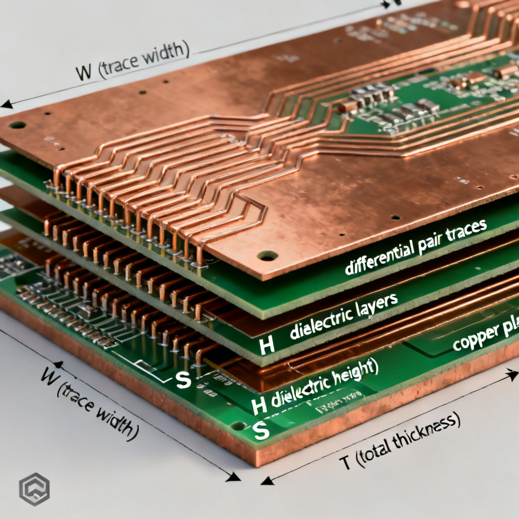
Trace Width (W) and Spacing (S)
Microstrip: To achieve 100Ω differential pair impedance with standard FR-4 (εr=4.2, H=4 mils), you typically need W≈5.5 mils and S≈7 mils. The spacing must be relatively large because the coupling is weak.
Stripline: For the same impedance, with the same dielectric height (H=8 mils total, 4 mils per side), you would need W≈4.5 mils and S≈5 mils. The traces are narrower and closer together due to stronger coupling.
Dielectric Height (H)
Microstrip: H is the distance from the trace to the nearest reference plane. Increasing H raises impedance. However, microstrip is sensitive to prepreg thickness variations.
Stripline: H is the total distance between the two planes. The trace position (centered or offset) dramatically affects impedance. Offset stripline (trace closer to one plane) requires a different, more complex formula.
Copper Thickness (T)
Microstrip: Thicker copper (e.g., 2 oz vs. 1 oz) lowers impedance because it increases capacitance. The effect is more pronounced in microstrip due to sidewall capacitance.
Stripline: The effect of copper thickness is less dramatic but still significant. Thicker copper in stripline can cause impedance drops of 2-4Ω if not compensated.
Solder Mask Effect (Microstrip Only)
Solder mask (εr ≈ 3.5-4.0) adds capacitance to microstrip traces, typically lowering impedance by 2-5Ω. This is not a factor for stripline. Always ask your fabricator to include solder mask in their microstrip impedance calculations.
4. Advanced Considerations: Field Solvers Are Mandatory
While the formulas above are excellent for initial estimation and understanding the physics, no production-quality PCB should rely solely on closed-form equations. The reasons are:
- Non-ideal geometries: Trapezoidal trace cross-sections (due to etching), glass weave effects, and resin-rich areas cause deviations.
- Frequency dependence: At multi-GHz speeds, the dielectric constant (εr) and loss tangent (tan δ) vary. The formulas assume a single frequency.
- Multiple dielectrics: High-speed boards often use hybrid stacks (e.g., FR-4 with Rogers laminates). The effective εr is a weighted average.
Industry Best Practice: Use a 2D field solver such as Polar Instruments Si9000, Altium Designer’s Layer Stack Manager, or Cadence Sigrity. These tools solve Maxwell’s equations for your exact stackup geometry, accounting for all real-world effects. They will produce impedance values that match actual fabricated boards within ±5%.
5. Common Mistakes and How to Avoid Them
| Common Mistake | Consequence for Differential Pair Impedance | Solution |
|---|---|---|
| Using microstrip formula for stripline | Impedance error > 10% | Always verify the topology in your calculator. |
| Ignoring solder mask on microstrip | Measured impedance 2-5Ω low | Request solder mask modeling from fabricator. |
| Assuming εr is constant across frequency | Impedance shifts at high speed | Use manufacturer’s Dk vs. frequency data. |
| Using edge-coupled formula for broadside couplers | Completely wrong result | Broadside (stacked) pairs require a separate formula. |
| Not accounting for glass weave effect | Impedance varies across the board | Use spread glass or rotate traces 10 degrees. |
6. Practical Stackup Recommendations for High-Speed PCBs
To achieve reliable differential pair impedance for both microstrip and stripline, follow these stackup guidelines:
For Microstrip Differential Pairs (Outer Layers)
- Minimum spacing rule: Keep S ≥ 2×H to avoid excessive coupling and manufacturing difficulty.
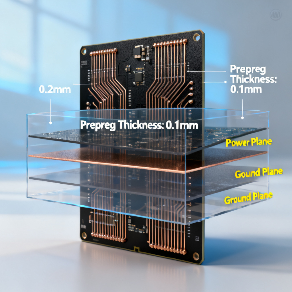
- Use a thin prepreg: H = 3-5 mils (0.076-0.127 mm) for fine-pitch routing.
- Include a solder mask compensation: Reduce trace width by 0.5-1 mil in your design to account for the mask.
- Avoid 90-degree bends: Use 45-degree chamfered or curved corners to maintain impedance continuity.
For Stripline Differential Pairs (Inner Layers)
- Use symmetric stripline whenever possible: It offers the best shielding and impedance control.
- Keep the trace centered: Offset by more than 20% will cause impedance asymmetry.
- Maintain a balanced stackup: Ensure the dielectric thickness above and below the pair is equal.
- Avoid crossing voids or splits in reference planes: This destroys the return path and causes impedance anomalies.
7. Conclusion: Choose the Right Formula for Your Layer
Following differential pair routing rules, note that the formulas for differential pair impedance are not interchangeable. Microstrip and stripline are fundamentally different electromagnetic structures. Using the wrong formula will lead to impedance mismatch, signal degradation, and potential product failure.
Final Checklist for Your Design:
- Identify the layer type (microstrip or stripline).
- Use the appropriate formula for initial estimation.
- Validate with a field solver (Polar, Altium, Cadence).
- Confirm with your PCB fabricator that they use the correct topology in their CAM tool.
- Request impedance test coupons on your panel to verify actual results.
By understanding and respecting these differences, you will achieve robust, high-speed performance in your PCB designs. For custom impedance-controlled PCB fabrication with tight tolerances (±5% or better), contact our engineering team. We specialize in high-speed, multi-layer boards with both microstrip and stripline requirements.
Frequently Asked Questions About Differential Pair Impedance
What is the main difference between microstrip and stripline for differential pair impedance?
The main difference is that microstrip has fields partially in air, requiring a formula with an effective dielectric constant and weaker coupling constants (0.48 and -0.96), while stripline has fields fully in dielectric, using stronger coupling constants (0.347 and -2.9). This directly affects how you calculate differential pair impedance for each topology.
Can I use the same formula for both microstrip and stripline differential pairs?
No, you cannot. Using the same formula for both will result in a 5-15Ω error in differential pair impedance. The formulas have different constants and exponents because the electromagnetic environments are fundamentally different.
Why does solder mask affect microstrip but not stripline differential pair impedance?
Solder mask adds capacitance to outer layer traces, lowering differential pair impedance by 2-5Ω. Stripline is fully embedded in dielectric, so solder mask has no effect. Always include solder mask in microstrip impedance calculations.
What tools should I use for accurate differential pair impedance calculation?
For production-quality results, use 2D field solvers like Polar Si9000, Altium Designer’s Layer Stack Manager, or Cadence Sigrity. These tools account for real-world effects and provide accuracy within ±5% of fabricated boards.
How do I choose between microstrip and stripline for high-speed differential pairs?
Microstrip offers faster propagation and easier access but higher EMI. Stripline provides superior shielding and more predictable differential pair impedance but slower signal speed. Choose based on your signal integrity and EMI requirements.