[rank_math_breadcrumb]
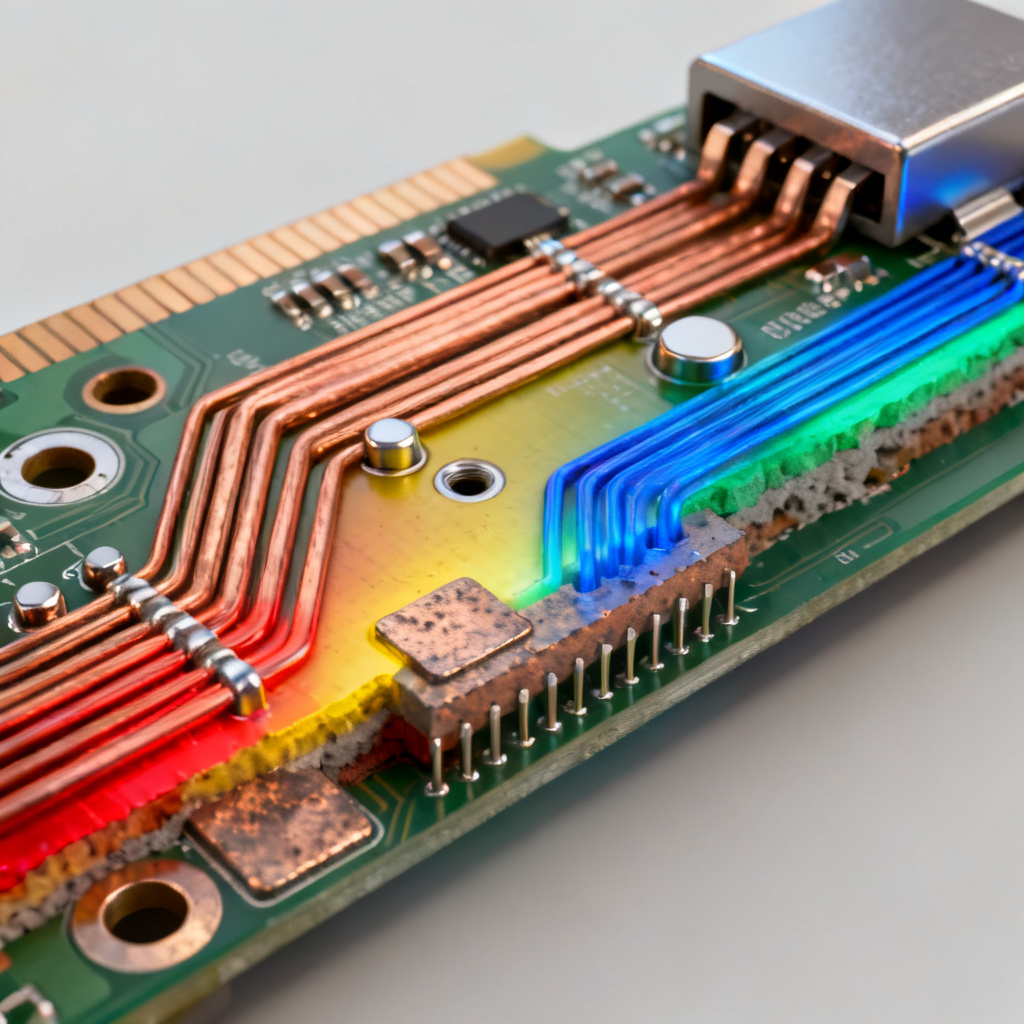
Differential pair impedance at discontinuities—specifically at vias, pads, and connectors—is a critical factor in high-speed PCB design, directly impacting signal integrity and data transmission reliability. This comprehensive guide explores the physics, modeling, and mitigation strategies for maintaining controlled impedance across these common discontinuity points, ensuring robust performance for designs operating at 10 Gbps and beyond.
Chapter 1: Fundamentals of Differential Pair Impedance
1.1 What is Differential Impedance?
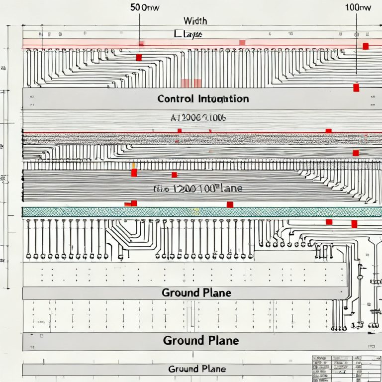
Differential pair impedance (Z_diff) is the impedance between the two conductors of a differential pair when driven by a differential signal (equal and opposite voltages). For a coupled microstrip or stripline pair, Z_diff is determined by trace width (W) and thickness (T), dielectric height (H) above the reference plane, edge-to-edge spacing (S) between the two traces, and dielectric constant (Dk) of the substrate. A typical target is 100Ω for USB, HDMI, and Ethernet, or 85Ω for some high-speed SerDes (e.g., PCIe Gen 4/5). The key principle is that the electromagnetic field is tightly coupled between the two traces, and any deviation in the physical structure disrupts this coupling, causing impedance mismatch.
1.2 The Nature of Discontinuities
A discontinuity is any point where the transmission line’s characteristic impedance changes abruptly. This can be due to geometric changes (e.g., via pads, antipads, connector footprints), material changes (e.g., solder mask over traces, air gaps near connectors), or stub effects (e.g., unused via barrels, connector tails). The impact is quantified by the reflection coefficient (Γ), which determines how much signal energy is reflected back toward the source. Even a 10% impedance mismatch can cause significant eye closure at high data rates.
Chapter 2: Vias – The Most Common Discontinuity
2.1 Why Vias Cause Impedance Disruption
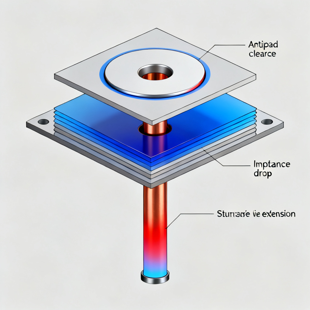
Vias are essential for routing signals between layers, but they introduce a complex impedance discontinuity. A via consists of a via barrel (the conductive cylinder), via pad (top and bottom layers), antipad (the clearance hole in the reference plane), and stub (the unused portion of the via barrel). The primary mechanism is capacitive loading: the via pad and barrel create increased capacitance relative to the reference plane, while the antipad creates an inductive effect. The net result is a local impedance drop, often from 100Ω down to 60–70Ω, depending on geometry.
2.2 Key Parameters Affecting Via Impedance
According to high-speed digital design principles, the impedance of a via is a function of pad diameter (larger pads increase capacitance, lowering impedance), antipad diameter (larger antipads reduce capacitance, raising impedance), via barrel diameter (larger barrels increase inductance, raising impedance), number of reference planes (multiple planes increase parallel capacitance, lowering impedance), and via length (longer vias have higher inductance, but also higher capacitance if multiple planes are present). For differential vias (pair of vias used for a differential signal), the pitch between the two vias is critical: a pitch that is too small increases mutual capacitance, while a pitch that is too large increases mutual inductance. The ideal pitch is typically 2–3 times the via diameter. The stub is the single most damaging element: a stub acts as a quarter-wave resonator, creating a deep null in the insertion loss at the frequency where the stub length equals λ/4. For 10 Gbps signals, even a 20-mil stub can cause a 3 dB loss. Backdrilling (removing the stub) is the most effective mitigation.
2.3 Modeling and Simulation of Via Impedance
Accurate modeling requires 3D electromagnetic (EM) simulation tools (e.g., Ansys HFSS, CST, Keysight ADS). Key steps include extracting S-parameters of the via structure (including pads, antipads, and stubs), converting to TDR (Time Domain Reflectometry) to visualize impedance vs. time, optimizing antipad size to achieve a target impedance (e.g., 100Ω) at the via location, and simulating differential pairs with both vias to account for coupling. A practical rule of thumb: for a standard 4-layer board with 0.062″ thickness, a via with 12-mil pad, 28-mil antipad, and 8-mil barrel will have ~85Ω impedance; adjust antipad to 32-mil to reach 100Ω.
2.4 Mitigation Strategies for Vias
Effective mitigation strategies for differential pair impedance at vias include: backdrilling to remove the stub (mandatory for signals above 5 Gbps); optimizing antipad size (use larger antipads to reduce capacitance, and for differential vias use a shared antipad—oval or rectangular—to reduce mutual coupling); adding ground vias adjacent to signal vias to provide a return path and reduce loop inductance (a rule of thumb is one ground via per two signal vias); reducing via count by minimizing layer transitions in high-speed paths (use blind or buried vias if possible); using microvias for HDI boards (lower parasitic capacitance due to small size); and matching differential via pairs to ensure identical geometry and stub lengths (asymmetry causes mode conversion, generating common-mode noise).
Chapter 3: Pads – The Overlooked Discontinuity
3.1 How Pads Affect Differential Impedance
Pads are the copper landing areas for component pins (e.g., BGA, QFN, connector pins) or test points. They are typically wider than the trace, creating a capacitive discontinuity. The pad acts as a small patch capacitor, lowering the local impedance. A typical BGA pad (e.g., 12-mil diameter) on a 100Ω differential pair can cause a 10–15% impedance drop, an effect more pronounced for smaller trace widths (e.g., 4-mil traces on fine-pitch BGAs). The solder mask over pads also changes impedance: solder mask has a higher dielectric constant (Dk ≈ 3.5–4.0) than air, which increases capacitance. Removing solder mask from high-speed pads (solder mask defined vs. non-solder mask defined) can improve impedance control by 2–5%.
3.2 Types of Pads and Their Impact
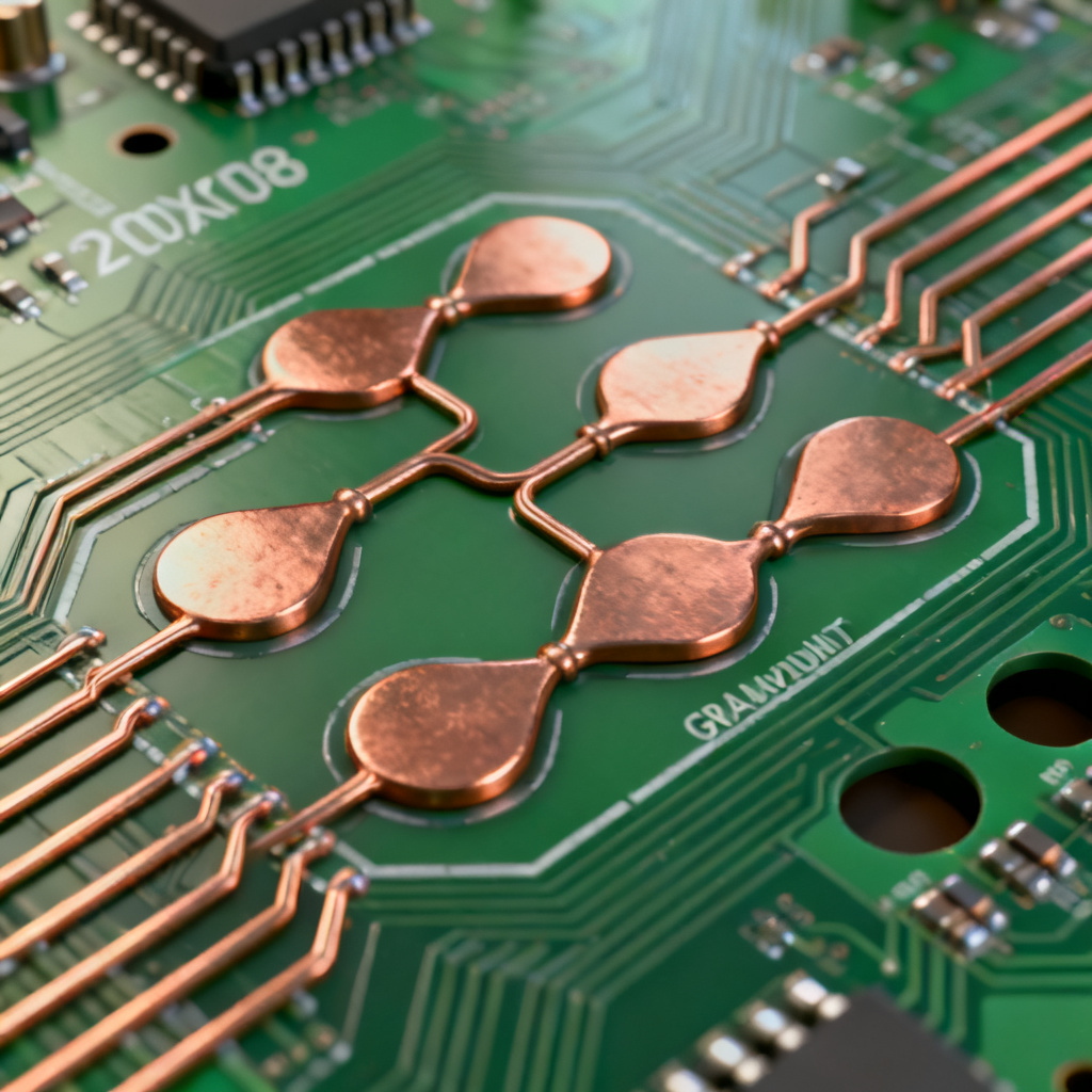
Different pad types have varying impedance impacts: circular pads (standard) cause a moderate drop of 5–10% (typical for BGA, QFN); teardrop pads cause minimal drop of less than 5% (used for via-to-trace transitions); test point pads (square) cause a large drop of 15–20% (used for debug headers); and connector footprint pads (rectangular) cause a significant drop of 10–20% (used for HDMI, USB connectors).
3.3 Mitigation Strategies for Pads
To manage differential pair impedance at pads, use teardrop pads to taper the trace into the pad, reducing capacitive loading and smoothing the impedance transition. Minimize pad size by using the smallest pad allowed by the fabrication process (for BGA, use solder mask defined (SMD) pads if the vendor supports it). Add ground cutouts by removing copper from the reference plane directly under the pad to reduce capacitance, especially effective for large connector pads. Use non-solder mask defined (NSMD) pads, which have no solder mask over the copper, reducing capacitance (though requiring tighter fabrication tolerances). Optimize trace width by slightly narrowing the trace near the pad to compensate for increased capacitance (impedance compensation). Simulate the pad-to-trace transition using 2.5D or 3D simulation to verify the impedance profile and adjust pad geometry iteratively. For differential pairs, ensure both pads have identical geometry to avoid common-mode noise, and avoid placing pads directly over a ground plane split.
Chapter 4: Connectors – The System-Level Discontinuity
4.1 Why Connectors Are Problematic
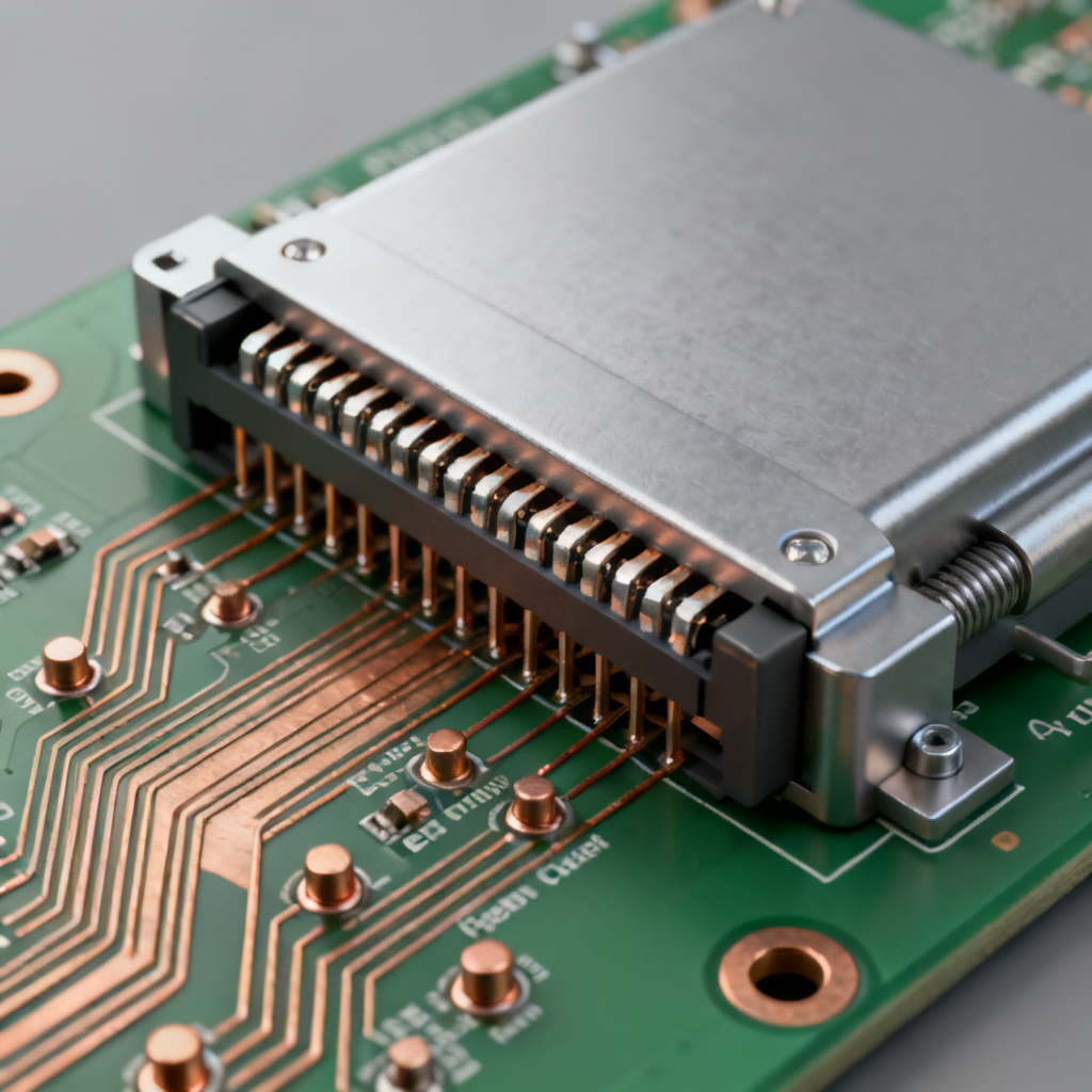
Connectors are the most complex discontinuity because they involve mechanical transitions (from PCB trace to connector pin to cable), multiple materials (copper, plastic housing, air gaps), long stubs (connector tails or solder pins), and impedance mismatch between PCB and cable (e.g., 100Ω PCB to 90Ω cable). A typical HDMI connector can have an impedance of 80–90Ω at the transition, causing a 10–20% mismatch. For PCIe Gen 4 (16 Gbps), this can cause a 3 dB insertion loss penalty. The connector footprint on the PCB is often the weakest link: large pads, long pins, and absence of a continuous reference plane create a severe discontinuity.
4.2 Key Parameters Affecting Connector Impedance
Key parameters include pin pitch (wider pitch increases inductance, raising impedance; typical pitch for high-speed connectors is 0.5 mm to 1.0 mm), pin length (longer pins increase inductance and stub effects; for vertical connectors, the pin stub below the PCB is often overlooked), housing material (plastic housing has a Dk of 2.5–4.0, affecting the effective dielectric constant), air gaps (air gaps around pins reduce effective Dk, increasing impedance, which can be beneficial or detrimental depending on design), and reference plane cutouts (connectors often require large cutouts for pin insertion, disrupting the return path).
4.3 Modeling and Simulation of Connector Impedance
Connectors require full 3D EM simulation due to their 3D geometry. Key steps include importing the connector 3D model from the manufacturer (e.g., Samtec, Molex, Amphenol), defining the PCB footprint (pads, antipads, trace transitions), simulating the entire path from PCB trace to connector pin to cable, and extracting TDR and S-parameters to identify impedance peaks and dips. Many connector manufacturers provide IBIS-AMI models or S-parameter files for their products, which should be used for system-level simulation.
4.4 Mitigation Strategies for Connectors
To maintain differential pair impedance at connectors, select high-speed rated connectors specifically designed for differential signaling (e.g., Samtec HDR, Molex SlimStack) with controlled impedance (typically 100Ω ±10%). Optimize the PCB footprint by following the manufacturer’s recommended footprint exactly, including pad size, antipad diameter, and ground via placement. Add ground vias around the connector near each signal pin to provide a low-inductance return path (a rule of thumb is one ground via per two signal pins). Use stitch vias for connectors with multiple ground pins by connecting them with a ground plane on the inner layer to reduce loop inductance. Minimize pin stub length by backdrilling unused pin tails for through-hole connectors, or ensuring minimal solder fillet for SMT connectors. Match PCB impedance to the connector by adjusting trace width and spacing to match the connector’s impedance (e.g., if the connector is 90Ω, design the PCB traces for 90Ω, not 100Ω). For critical paths, add series resistors (e.g., 0Ω or 10Ω) or AC coupling capacitors to absorb reflections, though this adds cost and complexity. Finally, simulate the entire channel including the PCB trace, via, connector, and cable in a single simulation, optimizing the transition using iterative tuning.
Chapter 5: Combined Effects and System-Level Optimization
5.1 The Cumulative Impact of Multiple Discontinuities
In a real PCB, a high-speed differential pair may encounter multiple vias, pads, and a connector. Each discontinuity adds a small impedance mismatch, and the cumulative effect can be severe. For example, a trace-to-via transition may cause a 10% mismatch, a via-to-pad transition a 5% mismatch, and a pad-to-connector transition a 15% mismatch, resulting in a total cumulative mismatch of 30%, causing significant eye closure and bit errors. The worst-case scenario is when discontinuities are spaced at half-wavelength intervals, causing constructive interference of reflections—common in multi-layer boards with multiple via transitions.
5.2 Design Rules for Minimizing Cumulative Effects
To minimize cumulative effects on differential pair impedance, minimize the number of discontinuities by using as few vias as possible and routing high-speed signals on the same layer when feasible. Space discontinuities evenly, avoiding clustering vias or pads—space them at least 5 times the trace width apart to reduce coupling. Use impedance compensation by adjusting trace width for short sections between discontinuities to compensate for the impedance drop, often done with a tapered transition. Simulate the entire path using a 3D EM simulator to model the entire channel from driver to receiver, optimizing each discontinuity iteratively. In the digital domain, use transmitters with pre-emphasis or receivers with continuous-time linear equalization (CTLE) to compensate for channel losses—a system-level solution.
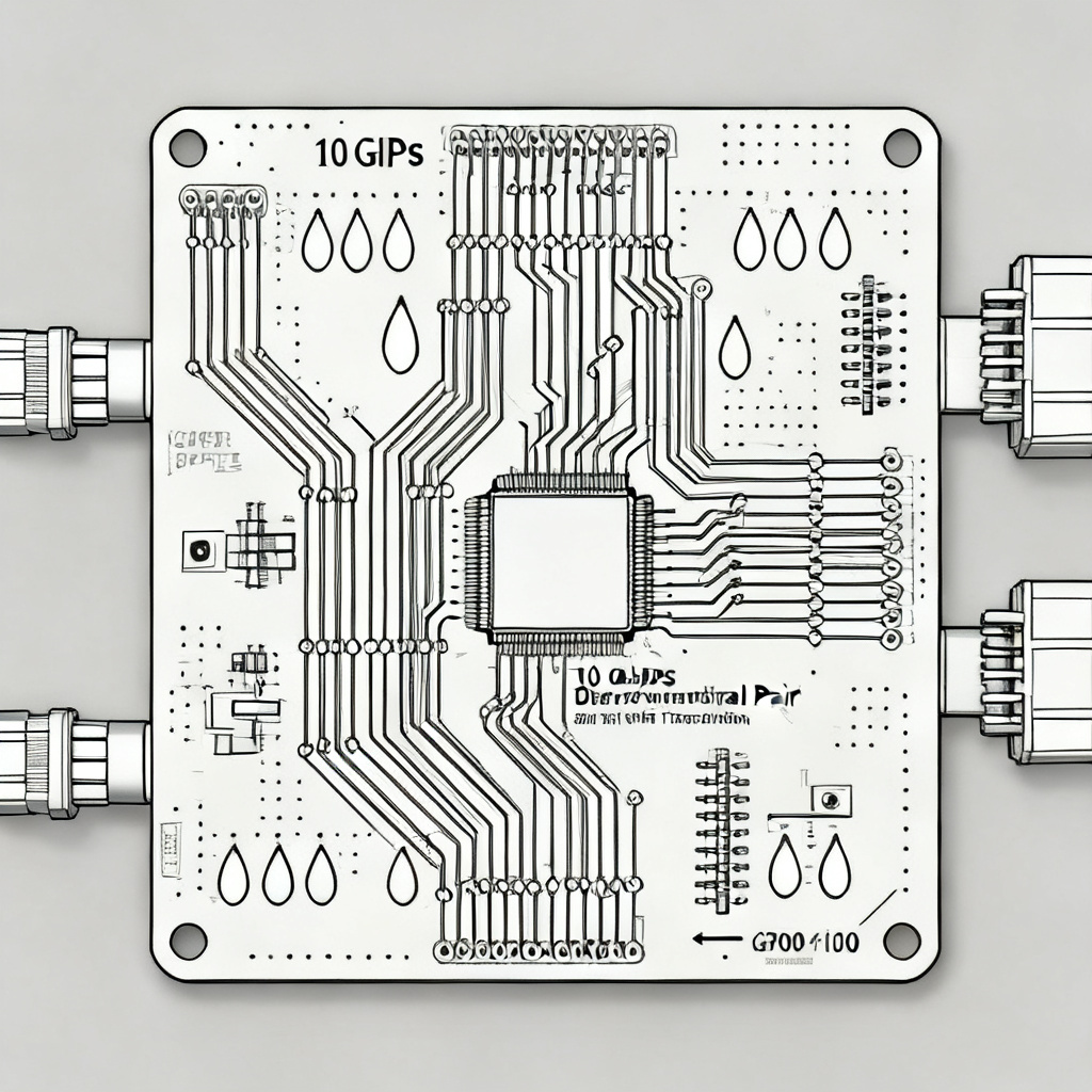
5.3 Practical Example: 10 Gbps Differential Pair Design
Consider a 10 Gbps differential pair (e.g., PCIe Gen 3) on a 6-layer board with two via transitions and a connector. Step 1: Design traces for 100Ω differential impedance (stripline, 5-mil width, 8-mil spacing, 4-mil dielectric height). Step 2: Optimize via antipad to 30-mil (for 100Ω) and use backdrilling to remove stubs. Step 3: Use teardrop pads for via-to-trace transitions; for BGA pads, use NSMD with 10-mil diameter. Step 4: Select a 100Ω-rated connector (e.g., Samtec HDR) and use the manufacturer footprint with ground vias every 2 signal pins. Step 5: Simulate the entire channel, adjusting trace width near the connector to match connector impedance (e.g., reduce width to 4.5 mils for 95Ω). Step 6: Measure TDR, targeting impedance within 90–110Ω at all points; if a dip is found, adjust antipad size or add a ground via.
Chapter 6: Measurement and Validation
6.1 TDR Measurement for Discontinuities
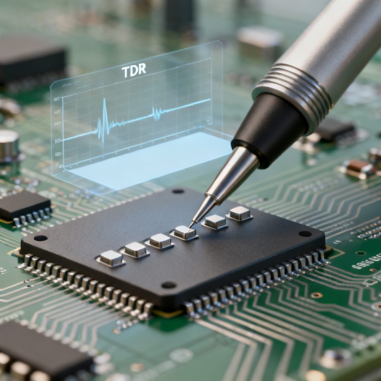
Time Domain Reflectometry (TDR) is the gold standard for measuring impedance discontinuities. A TDR sends a fast rise-time pulse (e.g., 35 ps) and measures reflections. Key steps: calibrate with open, short, and load standards; probe the differential pair at the driver end; identify impedance dips (capacitive discontinuities) and peaks (inductive discontinuities); measure the impedance at each discontinuity (via, pad, connector); and compare to the target (e.g., 100Ω ±10%). For differential pairs, use a differential TDR probe; single-ended TDR can be used but requires de-embedding of the common-mode component.
6.2 VNA Measurement for Frequency Domain
To verify compliance with differential pair routing rules, Vector Network Analyzer (VNA) measurements provide S-parameters, which can be converted to TDR. Key metrics include insertion loss (Sdd21) which should be flat with no deep nulls, return loss (Sdd11) which should be below -15 dB at the operating frequency, and mode conversion (Scd21) which should be below -30 dB to indicate good balance.
6.3 Common Measurement Pitfalls
Common pitfalls include probe loading (probes add capacitance, skewing results; use low-capacitance probes <0.1 pF), calibration errors (use a calibration substrate designed for differential signals), and temperature effects (impedance changes with temperature due to copper resistivity and dielectric Dk; measure at operating temperature).
Chapter 7: Advanced Topics and Future Trends
7.1 Beyond 25 Gbps: The Need for 3D Simulation
At data rates above 25 Gbps (e.g., 112 Gbps PAM4), even small discontinuities (e.g., a 2-mil pad) cause significant signal degradation. Designers must use full 3D EM simulation for every via, pad, and connector—simplified 2D models are insufficient.
7.2 Material Selection for High-Speed Discontinuities
Low-loss dielectrics (e.g., Rogers 4350B, Megtron 6) reduce dielectric absorption, which can exacerbate impedance mismatches. Copper roughness increases skin effect losses, which can mask impedance discontinuities; use smooth copper (e.g., RTF or VLP) for high-speed layers.
7.3 The Role of AI in Discontinuity Optimization
Emerging AI-based tools (e.g., from Cadence, Ansys) can automatically optimize via antipads, pad shapes, and connector footprints by running thousands of simulations, reducing design time from weeks to hours.
Best Practices for Differential Pair Impedance at Discontinuities
| Discontinuity Type | Key Mitigation Strategy | Simulation Required | Measurement Method |
|---|---|---|---|
| Vias | Backdrilling, optimized antipad, ground vias | 3D EM (HFSS, CST) | TDR, VNA |
| Pads | Teardrop, NSMD, impedance compensation | 2.5D (ADS, HyperLynx) | TDR |
| Connectors | High-speed rated, manufacturer footprint, ground vias | 3D EM (full model) | TDR, VNA |
Final Recommendations for PCB Designers
Simulate early, simulate often—use 3D EM simulation for all high-speed discontinuities. Minimize discontinuities by using fewer vias, smaller pads, and shorter connector stubs. Match impedance at every transition by adjusting trace width, antipad size, and pad geometry to maintain 100Ω ±10%. Validate with TDR on prototype boards to ensure impedance targets are met. Partner with manufacturers to work with PCB fabricators and connector vendors to get accurate models and fabrication tolerances. By following these guidelines, you can achieve robust signal integrity for differential pairs operating at speeds up to 28 Gbps and beyond, ensuring reliable data transmission in your next high-speed PCB design.
FAQ: Differential Pair Impedance at Discontinuities
What is differential pair impedance at discontinuities?
Differential pair impedance at discontinuities refers to the deviation from the target impedance (e.g., 100Ω) caused by physical structures like vias, pads, and connectors in a high-speed PCB. These variations lead to signal reflections, jitter, and data errors.
How do vias affect differential pair impedance?
Vias introduce capacitive loading from pads and barrels, along with inductive effects from antipads, causing a local impedance drop. The stub (unused barrel portion) acts as a quarter-wave resonator, creating significant signal loss at specific frequencies.
What are the best ways to mitigate impedance discontinuities at connectors?
Use high-speed rated connectors with controlled impedance, optimize the PCB footprint per manufacturer guidelines, add ground vias near signal pins, minimize pin stub length, and simulate the entire channel from PCB trace to cable.
Why are pads considered an overlooked discontinuity?
Pads are wider than traces, creating capacitive loading that lowers impedance. Solder mask over pads further increases capacitance. Teardrop pads, non-solder mask defined (NSMD) pads, and ground cutouts help mitigate these effects.
What measurement methods are used to validate differential pair impedance?
TDR (Time Domain Reflectometry) provides time-domain impedance profiles, while VNA (Vector Network Analyzer) measures frequency-domain S-parameters. Both methods are essential for validating impedance at discontinuities like vias, pads, and connectors.