[rank_math_breadcrumb]
Master differential pair impedance calculation using Polar Si9000 with this comprehensive guide. This step-by-step tutorial covers stackup setup, field solver configuration, edge-coupled vs. broadside models, and common errors—essential for high-speed PCB designers and B2B buyers seeking controlled impedance manufacturing.

1. Understanding Differential Pair Impedance Basics
Differential pair impedance calculation using Polar Si9000 begins with fundamental concepts. Differential impedance (Zdiff) is the impedance between two conductors when driven by a differential signal. It is not simply twice the single-ended impedance—for edge-coupled microstrip, Zdiff ≈ 2 × Z0 × (1 – 0.48 × e^(-0.96 × s/h)).
Key Parameters Affecting Zdiff
Critical variables in differential pair impedance calculation using Polar Si9000 include trace width (W), trace spacing (S), dielectric thickness (H), dielectric constant (Er), and copper thickness (T). Wider traces lower Zdiff; tighter spacing increases coupling and lowers Zdiff; thicker dielectric increases Zdiff; higher Er lowers Zdiff.
Common Target Impedances
USB 2.0/3.0 targets 90Ω differential; HDMI, DisplayPort, and Ethernet target 100Ω; PCIe Gen 3/4 targets 85Ω (sometimes 100Ω). Accurate differential pair impedance calculation using Polar Si9000 ensures these specifications are met.
2. Selecting the Correct Polar Si9000 Model
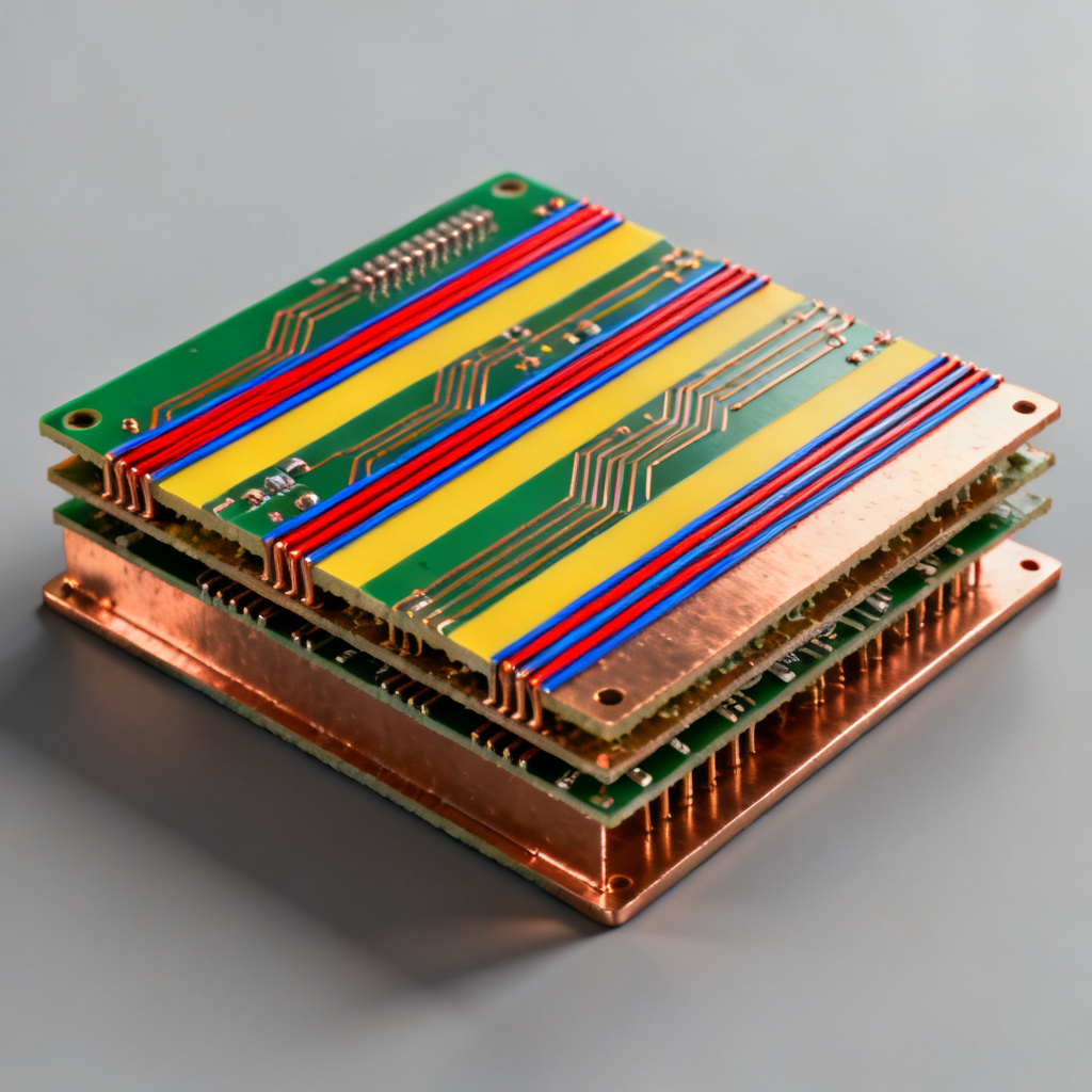
Differential pair impedance calculation using Polar Si9000 requires choosing the right field solver model. For outer layers, use Edge-Coupled Microstrip (1B) or Edge-Coupled Coated Microstrip (with solder mask). For inner layers, use Edge-Coupled Stripline (1B1A) or Offset Stripline. For stacked traces on adjacent layers, use Broadside Coupled Stripline.
Edge-Coupled Microstrip for Outer Layers
This model is most common for high-speed connectors. Input trace width, spacing, dielectric height to ground, and copper thickness. The coated version accounts for solder mask effects, which lower impedance slightly.
Edge-Coupled Stripline for Inner Layers
Use this when the pair is sandwiched between two reference planes. It offers best isolation for backplanes. Offset stripline applies when the pair is closer to one plane than the other.
Broadside Coupled Stripline for Stacked Traces
Less common but used in dense designs where traces overlap vertically. Spacing here means vertical dielectric thickness between layers.
3. Setting Up Stackup Parameters
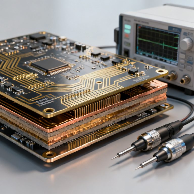
Accurate differential pair impedance calculation using Polar Si9000 depends on correct stackup input. Define dielectric layers (core vs. prepreg), specify material Er at operating frequency, and enter dielectric height from reference plane to trace layer. Copper thickness must be finished thickness after plating.
Trace Geometry Input
Enter trace width (W), edge-to-edge spacing (S), and trace thickness (T). Both traces in a pair typically have identical width. For coated microstrip, add solder mask thickness (0.5–1.0 mils) and its Er (3.5–4.0).
Target Impedance Setting
In the target field, enter desired Zdiff (e.g., 100Ω). Polar Si9000 can solve for required trace width and spacing using synthesis mode.
4. Running the Field Solver and Interpreting Results
Click “Solve” after entering parameters. Differential pair impedance calculation using Polar Si9000 outputs Zdiff, single-ended impedance Z0, propagation delay, and coupling coefficient K. For example, with 6 mil width, 6 mil spacing, 4 mil dielectric, Er 4.2, and 1 oz copper, Zdiff ≈ 98.7Ω (close to 100Ω target). Adjust spacing to 5.8 mils or width to 5.9 mils for exact 100Ω.
Synthesis vs. Analysis Mode
In line with differential pair routing rules, synthesis mode calculates the required trace width (W) and spacing (S) based on target differential impedance (Zdiff), while analysis mode computes the actual Zdiff using fixed W and S. Use synthesis mode for initial design and analysis mode for post-design verification.
5. Advanced Tips and Common Pitfalls
Even experienced designers miss nuances in differential pair impedance calculation using Polar Si9000. Ignoring adjacent traces, using incorrect Er at high frequencies, forgetting return current path continuity, and misinterpreting spacing in broadside models are common errors.
Frequency-Dependent Er
FR-4 Er drops from 4.2 at 1 GHz to 3.8 at 10 GHz. Use frequency-dependent Er in Polar Si9000 for accuracy.
Stackup Editor for Multi-Layer Boards
The Stackup Editor defines multiple layers and calculates impedance for all differential pairs simultaneously, saving time in complex designs.
6. Exporting Results and Sharing with Manufacturer
Export a report (PDF or CSV) from Polar Si9000 including stackup details, trace geometry, calculated Zdiff and Z0, frequency, and temperature assumptions. Send the .stack file or a clear note specifying target impedance, model used, and material parameters. Tolerance is typically ±10% (±5% for premium).
7. Verifying Impedance with TDR
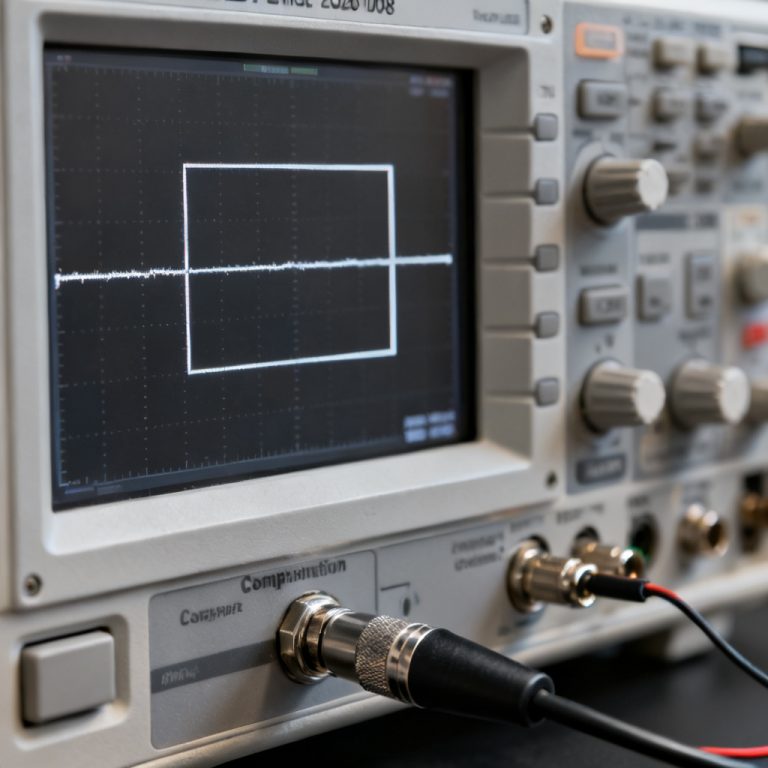
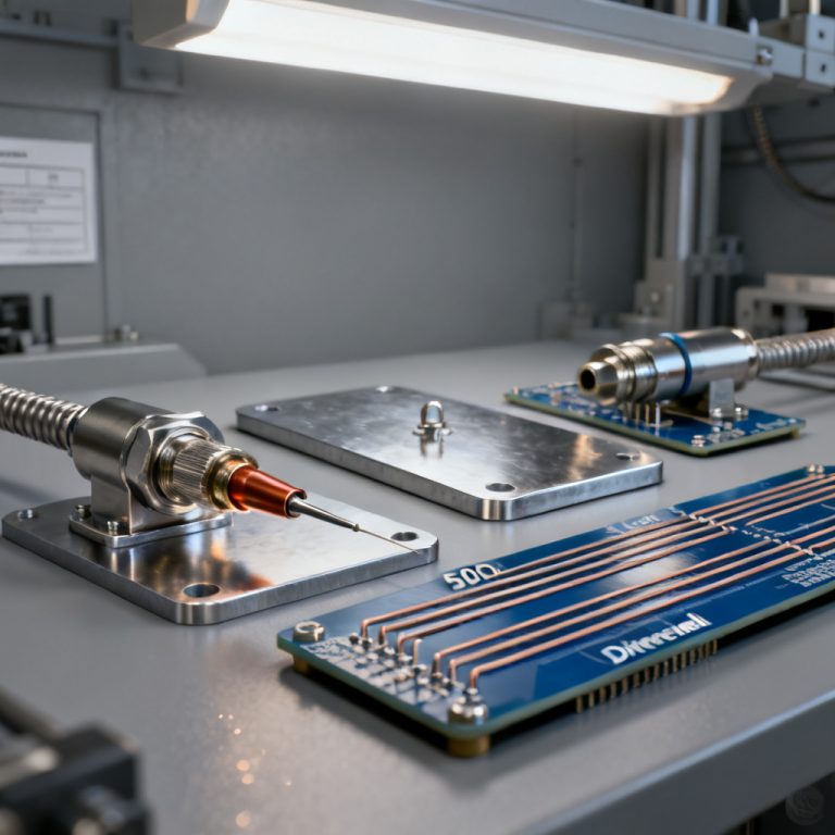
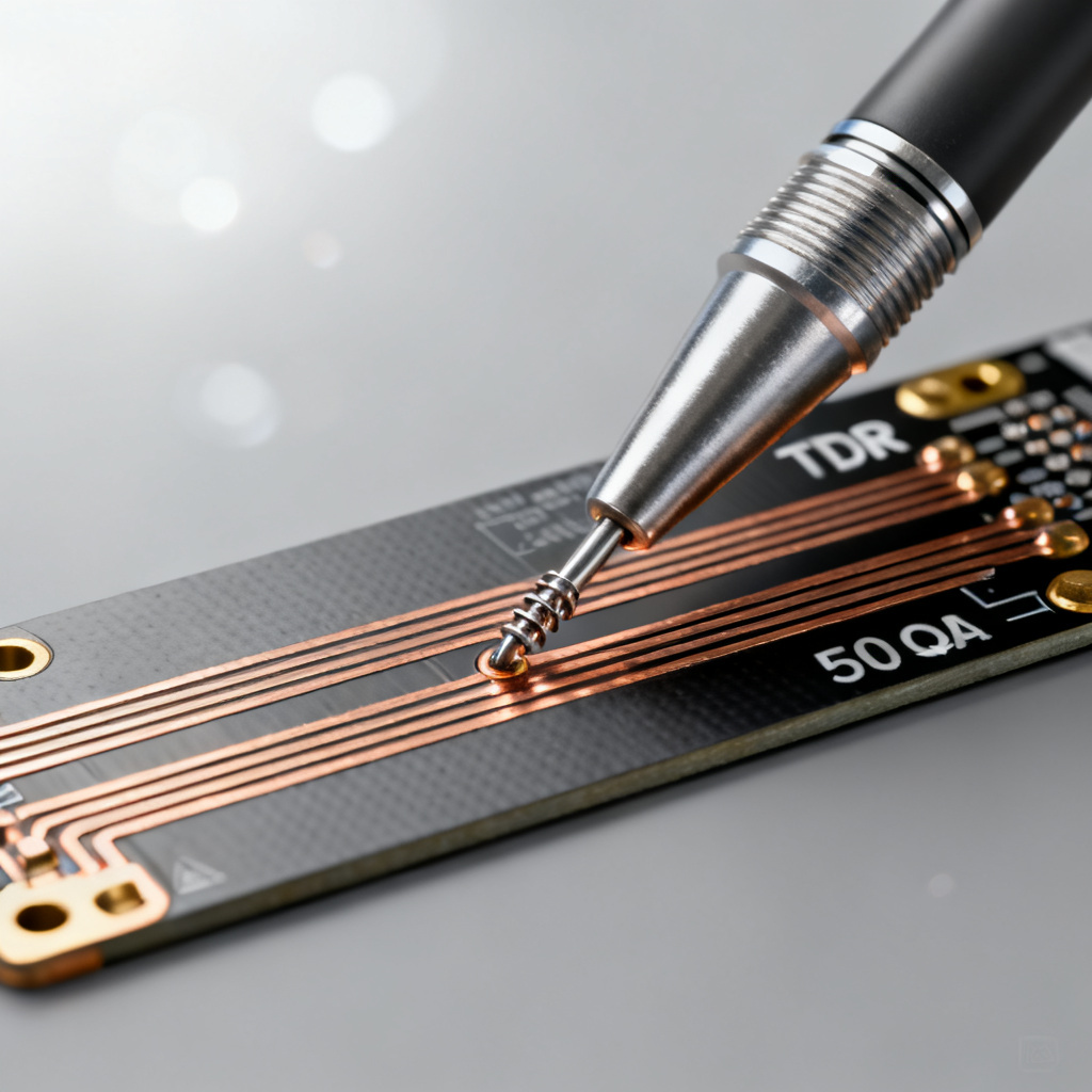
While differential pair impedance calculation using Polar Si9000 is theoretical, TDR testing verifies actual impedance. Compare TDR-measured Zdiff to target. If 5% lower, check dielectric thickness, copper etching, or solder mask effects. Our factory offers TDR testing with reports matching your Polar Si9000 file.
Conclusion: Reliable High-Speed PCB Design
Follow these steps for accurate differential pair impedance calculation using Polar Si9000: choose correct model, input stackup parameters, run solver, adjust trace width/spacing, export results, and verify with TDR. This ensures signal integrity, reduces development time, and builds trust with your PCB supplier.

Frequently Asked Questions
What is differential pair impedance calculation using Polar Si9000?
It is the process of using Polar Si9000 field solver to compute the differential impedance (Zdiff) of a pair of traces, ensuring controlled impedance for high-speed signals.
Why is differential pair impedance calculation using Polar Si9000 important?
Accurate calculation prevents signal integrity issues like reflections, crosstalk, and timing errors in high-speed interfaces such as USB, HDMI, and PCIe.
What models are used in differential pair impedance calculation using Polar Si9000?
Common models include Edge-Coupled Microstrip, Edge-Coupled Stripline, Offset Stripline, and Broadside Coupled Stripline, selected based on layer position and coupling type.
How do I verify results from differential pair impedance calculation using Polar Si9000?
Verify using TDR (Time Domain Reflectometry) testing, comparing measured Zdiff to the calculated target. Our factory provides TDR reports for all high-speed orders.
Can I share my Polar Si9000 file with a manufacturer?
Yes, export a .stack file or PDF report including all parameters. This ensures the manufacturer can replicate your stackup and impedance targets.
Differential Pair Impedance Parameters Table
| Parameter | Description | Impact on Differential Pair Impedance Calculation |
|---|---|---|
| Trace Width (W) | Width of each conductor in the pair | Wider traces lower Zdiff |
| Trace Spacing (S) | Edge-to-edge distance between traces | Tighter spacing increases coupling, lowers Zdiff |
| Dielectric Height (H) | Distance from trace to reference plane | Thicker dielectric increases Zdiff |
| Dielectric Constant (Er) | Material permittivity at operating frequency | Higher Er lowers Zdiff |
| Copper Thickness (T) | Finished copper thickness after plating | Thicker copper slightly lowers Zdiff |
Comparison: Our High-Speed PCB Services vs. Standard PCB Suppliers
Our factory specializes in controlled impedance manufacturing with tolerance ±5%, accepting Polar Si9000 .stack files directly. Standard suppliers often offer ±10% tolerance and may not support custom stackup files. We provide TDR testing reports for every high-speed order, ensuring your differential pair impedance calculation using Polar Si9000 matches production reality.
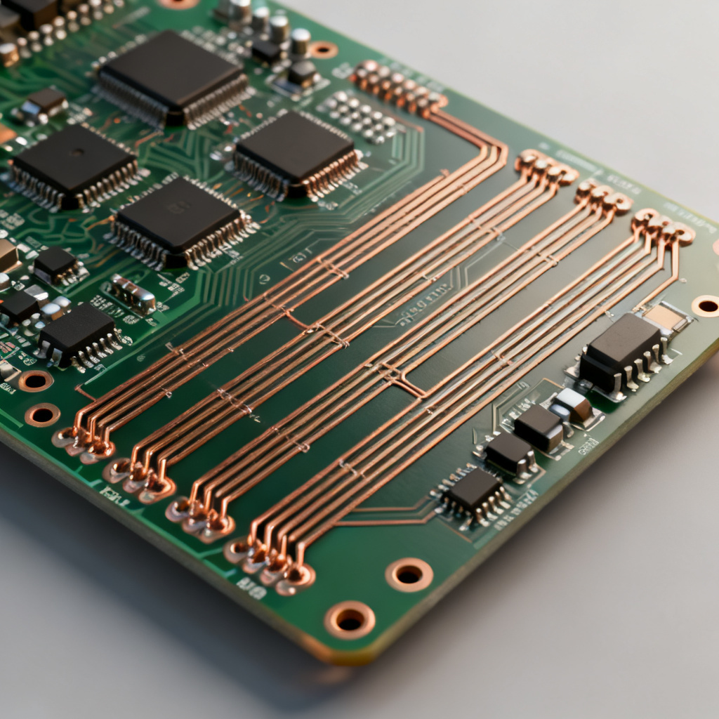
Expert Glossary for Differential Pair Impedance Calculation
Differential impedance (Zdiff): The impedance between two conductors driven by a differential signal. Odd-mode impedance (Zodd): Half of Zdiff, used in coupling analysis. Coupling coefficient (K): Measures how tightly traces are coupled; K > 0.5 indicates strong coupling. Time Domain Reflectometry (TDR): A measurement technique that sends a fast pulse to detect impedance discontinuities.