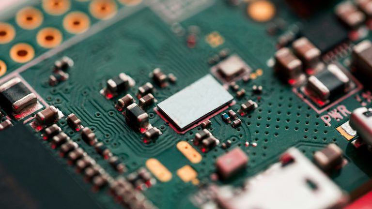
Panasonic Megtron series has long been recognized as the global industry benchmark for high-speed digital PCB dielectric materials, covering Megtron 4, Megtron 6, and Megtron 8 three mainstream grades. With low dissipation factor (low Df), stable dielectric constant (Dk), high Tg, excellent CAF resistance and precise thickness consistency, megtron high speed pcb material perfectly solves signal attenuation, insertion loss, impedance deviation and long-term reliability challenges in high-frequency high-speed transmission. Understanding megtron high speed pcb material is essential for modern high-speed digital design.
This full pillar guide integrates official Panasonic original specifications, professional high-speed engineering design experience and PCB manufacturing practical experience. As covered in our PCB Materials Selection Guide, mastering megtron high speed pcb material selection is critical for AI server and data center projects. It systematically explains Megtron series technical principles, product evolution, detailed parameter comparison, independent grade analysis, Megtron 6 vs Megtron 8 selection, manufacturing processing notes, application matching and engineering selection suggestions.
Table of Contents
- 1. Why Megtron Series Dominates Modern High-Speed Digital PCB
- 2. Panasonic Megtron Series Overview & Generation Evolution
- 3. Core Technical Parameters Explained: Dk, Df, Tg, CAF Resistance
- 4. Megtron 4 – Classic Low-Loss Entry-Level High-Speed PCB Material
- 5. Megtron 6 – Industry Standard for 25Gbps ~ 56Gbps Digital Design
- 6. Megtron 8 – Ultra-Low Loss Flagship for 112G PAM4 & 800G/1.6T Data Center
- 7. Megtron 6 vs Megtron 8: Performance, Cost & Application Full Comparison
- 8. Manufacturing & Processing Considerations for Megtron 4/6/8 PCB
- 9. Megtron Series Material Selection Guide by Application & Signal Rate
- 10. Key Takeaways
- 11. FAQ About Panasonic Megtron High-Speed PCB Material
- 12. Get Free Megtron Material Selection & Stackup Evaluation Support
Why Megtron Series Dominates Modern High-Speed Digital PCB
With the rapid iteration of AI computing, cloud data centers, 5G communication and 400G/800G optical communication infrastructure, traditional ordinary FR4 materials can no longer meet the signal integrity requirements of high-speed serial signals above 10Gbps. Signal insertion loss, dielectric loss, copper foil skin effect loss, layer warpage and CAF failure have become major pain points in high-speed PCB design. This is why megtron high speed pcb material has become the industry standard for high-speed digital applications. For a complete understanding of how material selection fits into the broader signal integrity picture, see our Signal Integrity Guide.
The core competitive advantages of megtron high speed pcb material include:
- Ultra-stable low Dk and low Df at high frequency, effectively suppressing high-frequency signal attenuation
- High glass transition temperature (high Tg), excellent thermal stability and anti-delamination capability
- Outstanding CAF (Conductive Anodic Filament) resistance, suitable for high-density fine via multilayer PCB
- Strict laminate and prepreg thickness tolerance, ensuring accurate impedance control
- Good compatibility with conventional PCB processes, supporting hybrid lamination with ordinary FR4
- Complete product grade coverage, from 10G entry-level to 112G PAM4 ultra-high-speed scenarios
Megtron high speed pcb material is widely deployed in AI server motherboards, data center switches and backplanes, 400G/800G optical modules, 5G base station high-speed boards and industrial high-speed control equipment, becoming the preferred standard material for modern high-speed digital hardware design.
Panasonic Megtron Series Overview & Generation Evolution
Panasonic continuously iterates Megtron material formula, glass weave structure and resin system according to the upgrade of communication bandwidth and signal rate. Megtron 4, Megtron 6 and Megtron 8 form a clear performance gradient, covering low-loss to ultra-low-loss full application scenarios. The evolution logic of megtron high speed pcb material is highly aligned with industry bandwidth upgrade.
Megtron Series Core Grade Overview Table
| Model | Loss Grade | Typical Working Frequency | Supported Signal Rate | Main Application Orientation |
|---|---|---|---|---|
| Megtron 4 | Standard Low-Loss | 10GHz | ≤10Gbps | 10G Ethernet, base station auxiliary board, industrial high-speed control |
| Megtron 6 | Advanced Low-Loss | 10GHz~14GHz | 10Gbps ~ 56Gbps | PCIe 4.0/5.0, 25G/56G SerDes, 400G optical module, AI server |
| Megtron 8 | Ultra-Low Loss | 10GHz+ | 56G NRZ / 112G PAM4 | 800G optical module, 112G SerDes backplane, hyperscale data center |
Each generation of megtron high speed pcb material optimizes resin composition and matches low-roughness copper foil, achieving lower dielectric loss while maintaining manufacturability and long-term reliability.
Core Technical Parameters Explained: Dk, Df, Tg, CAF Resistance
To correctly select and use megtron high speed pcb material, engineers must understand four core indicators that determine high-speed performance. The impact of these parameters on characteristic impedance is detailed in our Impedance Matching Ultimate Guide, which explains how Dk directly affects impedance calculation and tolerance.
Dk (Dielectric Constant)
Refers to the dielectric constant of the material, directly affecting signal transmission velocity and impedance design stability. The lower and more stable the Dk in high frequency, the smaller the signal delay deviation. Megtron high speed pcb material maintains flat Dk value across broadband, avoiding impedance mutation caused by frequency drift.
Df (Dissipation Factor)
Also called loss tangent, it is the key index of dielectric loss. The smaller the Df, the less high-frequency signal attenuation. It is the core difference between Megtron 4/6/8 three grades of megtron high speed pcb material.
Tg (Glass Transition Temperature)
High Tg material can withstand multiple reflow and high-temperature lamination, reducing board warpage, layer delamination and dimensional deformation, which is essential for multilayer high-density PCB.
CAF Resistance
Conductive Anodic Filament is a common failure mode of high-density PCB under high temperature and humidity. Megtron high speed pcb material is optimized in resin and glass fiber bonding to effectively prevent ion migration between vias and improve long-term service life of equipment.
Megtron 4 – Classic Low-Loss Entry-Level High-Speed PCB Material
Megtron 4 is Panasonic’s classic entry-level low-loss high-speed laminate, positioned as a cost-effective workhorse for low-to-medium high-speed digital design. It serves as the entry point to megtron high speed pcb material for cost-sensitive projects.
Key Performance Parameters
- Typical Df: 0.008–0.010 @10GHz
- Balanced low-loss performance with excellent conventional FR4 process compatibility
- Enhanced CAF resistance design, suitable for dense via multilayer boards
- High Tg formula resists thermal deformation during soldering and lamination
Main Application Scenarios
- 10G Ethernet switching boards
- 5G macro base station high-speed auxiliary boards
- Industrial automation high-speed control PCB
- Cost-sensitive consumer and communication high-speed equipment
Megtron 4 does not need over-engineering configuration for scenarios below 10Gbps signal rate. This grade of megtron high speed pcb material balances performance, cost and production yield perfectly.
Megtron 6 – Industry Standard for 25Gbps ~ 56Gbps Digital Design
Megtron 6 is currently the absolute mainstream standard material in the global high-speed PCB industry, dominating 25G to 56Gbps mass production projects of AI servers, data centers and optical modules. This grade of megtron high speed pcb material is the workhorse for most high-speed digital designs.
Core Electrical Parameters
- Dk: 3.4–3.7 (stable at high frequency band)
- Df: 0.002–0.005 @10GHz
- Ultra-low insertion loss, stable impedance control, excellent stackup consistency
Technical & Process Advantages
- Optimized symmetrical glass weave structure, reducing signal skew
- Strict thickness tolerance, convenient multilayer stackup design
- Compatible with standard PCB manufacturing process, no special complex process required
- Support hybrid lamination with ordinary FR4 to reduce overall board cost
Typical Application
- PCIe 4.0 / PCIe 5.0 high-speed channel routing
- 25G / 56G SerDes data center backplane interconnection
- 100G / 400G optical module carrier board
- Mainstream rack-mounted AI server motherboards and accelerator cards
For most high-speed digital designs between 10G and 56Gbps, Megtron 6 is the optimal megtron high speed pcb material solution with balanced performance, cost, manufacturability and supply stability.
Megtron 8 – Ultra-Low Loss Flagship for 112G PAM4 & 800G/1.6T Data Center
With the large-scale commercialization of 800G optical modules and 112G PAM4 high-speed interconnection, traditional low-loss materials represented by Megtron 6 can no longer meet the strict loss budget of long-channel high-speed signals. Megtron 8 is Panasonic’s top ultra-low-loss flagship material developed for next-generation ultra-high-speed scenarios, representing the pinnacle of megtron high speed pcb material technology.
Core Performance Advantages
- Ultra-low Df: less than 0.002 @10GHz, minimizing high-frequency signal attenuation
- Adopts advanced modified resin and ultra-fine symmetrical glass weave
- Default matching HVLP (High-Volume Low-Profiled) ultra-low roughness copper foil, greatly reducing skin effect loss
- Excellent high-frequency stability, suitable for long-distance backplane routing
Main Application Scenarios
- 800G coherent / non-coherent optical module high-speed PCB
- 112G SerDes data center high-speed backplane
- Hyperscale cloud computing data center interconnection board
- High-end network switching equipment with ultra-strict bit error rate requirements
Megtron 8 is not only a material upgrade, but also the core material foundation for data center bandwidth upgrading to 1.6T and above. This megtron high speed pcb material is the only mature mass-producible ultra-low-loss choice for 112G PAM4 design at present.
Megtron 6 vs Megtron 8: Performance, Cost & Application Full Comparison
Designers and buyers often face the choice between Megtron 6 and Megtron 8. The stack-up design principles covered in our Stackup Design Guide must account for the material differences when selecting megtron high speed pcb material. The following comprehensive comparison helps quick decision-making:
| Comparison Factor | Megtron 6 | Megtron 8 |
|---|---|---|
| Loss Level | Advanced Low-Loss | Ultra-Low Loss |
| 10GHz Df Range | 0.002–0.005 | <0.002 |
| Max Supported Rate | Stable up to 56Gbps NRZ | 56G NRZ / 112G PAM4 |
| Relative Cost | Baseline standard cost | 30%–50% higher than Megtron 6 |
| Manufacturing Difficulty | Standard process, high factory compatibility | Need precise lamination, etching and process control |
| Best Fit Scenario | Mass production 25G–56G projects, cost-sensitive | 800G/112G PAM4 ultra-high-speed mandatory projects |
Selection Principle
- Within 56Gbps, limited budget and conventional process: choose Megtron 6
- 800G optical module, 112G PAM4 channel, strict loss budget long backplane: must choose Megtron 8
- Transition projects can adopt hybrid stackup of Megtron 6 + Megtron 8 to balance performance and cost
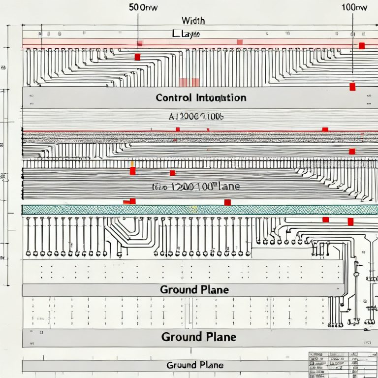
Manufacturing & Processing Considerations for Megtron 4/6/8 PCB
Although megtron high speed pcb material has good process compatibility with mainstream PCB production, standardized operation is required to guarantee yield, electrical performance and reliability.
Drilling Process
Adapt to standard mechanical drilling and laser drilling. Control drilling speed and tool wear to ensure smooth hole wall, avoid resin smearing and glass fiber burrs, so as to guarantee subsequent metallization and CAF resistance.
Lamination & Hybrid Stackup
All Megtron grades support hybrid lamination with ordinary FR4. Need to match Tg and thermal expansion coefficient of different materials to prevent layer delamination, warpage and thermal stress deformation.
Copper Foil Matching
- Megtron 4: adopt conventional standard copper foil to control cost
- Megtron 6 / Megtron 8: recommended HVLP ultra-low roughness copper foil, effectively reduce high-frequency skin effect loss and improve signal integrity
Material Storage & Moisture Proof
Megtron laminates and prepregs need dry constant temperature storage. Moisture absorption will cause bubbling and delamination during high-temperature lamination, and lead to drift of Dk/Df parameters. Strict moisture-proof management is required before production.
Megtron Series Material Selection Guide by Application & Signal Rate
When applying megtron high speed pcb material to your project, the high-speed routing rules in our High-Speed PCB Routing Rules guide should be coordinated with material selection. Quick selection standard for engineering projects:
| Signal Rate / Application | Recommended Megtron Grade |
|---|---|
| ≤10Gbps / Industrial control / 10G Ethernet | Megtron 4 |
| PCIe 4.0/5.0 / 25G~56G SerDes / AI server mainstream board | Megtron 6 |
| 400G optical module / 56G PAM4 medium and high-speed design | Prefer Megtron 6; evaluate Megtron 8 if loss budget tight |
| 800G optical module / 112G PAM4 backplane / 1.6T data center | Megtron 8 mandatory |
Following this rule can avoid over-specification cost waste and under-specification signal integrity failure, realizing precise matching of megtron high speed pcb material to project demand.
Key Takeaways
- Panasonic megtron high speed pcb material Megtron 4/6/8 forms a complete high-speed PCB material system, covering 10G to 112G PAM4 full scenario demands
- Megtron 4 is the cost-effective entry-level choice for below 10Gbps industrial and communication equipment
- Megtron 6 is the industry standard for 25G–56Gbps, with balanced performance, cost and process friendliness
- Megtron 8 is the ultra-low-loss flagship, exclusively for 800G/112G PAM4 next-generation data center and optical module design
- Megtron series supports FR4 hybrid lamination, which can optimize stackup structure and reduce overall board cost
- Correct copper foil selection, standardized drilling and lamination process are the key to give full play to megtron high speed pcb material performance
FAQ About Panasonic Megtron High-Speed PCB Material
Q1: What is the main difference between Megtron 4, Megtron 6 and Megtron 8?
Mainly reflected in Df loss value, supported signal rate, cost and manufacturing difficulty. The higher the grade, the lower the loss, the higher the supported rate, and the higher the cost and process requirement. This is the fundamental distinction in megtron high speed pcb material grades.
Q2: Can Megtron 6 replace Megtron 4 directly?
Yes in performance, but Megtron 6 cost is higher. For ≤10Gbps low-speed scenarios, Megtron 4 is more cost-effective without over-engineering when selecting megtron high speed pcb material.
Q3: Is Megtron material compatible with ordinary FR4 hybrid pressing?
Yes, all Megtron 4/6/8 support hybrid lamination with FR4, which is a common cost-saving design method in engineering when using megtron high speed pcb material.
Q4: Do I have to use HVLP copper foil for Megtron 8?
Suggested mandatory matching. Ordinary rough copper foil will produce large skin effect loss at 112G PAM4, resulting in excessive bit error rate when working with this premium megtron high speed pcb material.
Q5: Which Megtron grade should I choose for 400G optical module PCB?
Most 400G projects adopt Megtron 6 stably; only ultra-long channel and strict loss budget projects need to upgrade to Megtron 8 for optimal megtron high speed pcb material performance.
Get Free Megtron Material Selection & Stackup Evaluation Support
Are you designing AI server motherboards, 400G/800G optical modules, data center backplanes or high-speed communication PCB, and confused about megtron high speed pcb material grade selection, multilayer stackup design, Dk/Df parameter matching or insertion loss budget evaluation? Our team specializes in megtron high speed pcb material selection for high-speed digital projects.
We offer: Free Megtron 4/6/8 material grade selection consultation • Custom high-speed PCB layer stackup design & impedance simulation • Insertion loss signal integrity evaluation • Manufacturing process feasibility & cost optimization suggestion
Leave your project application scenario, signal rate requirement and board layer demand. We will reply with professional tailored Megtron material solution and quotation support as soon as possible.
About HighSpeedPCBs.com
We are a specialized PCB design and manufacturing service provider serving industrial, automotive, medical, and communications OEMs worldwide. Our expertise in megtron high speed pcb material selection ensures your high-speed digital designs perform reliably. Return to the PCB Materials Selection Guide for more coverage of material properties, selection criteria, and design guidelines.
© 2026 HighSpeedPCBs.com — Professional High-Speed PCB Solutions