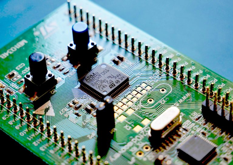
In modern high-speed electronics—including 5G communication, servers, AI hardware, medical devices, and wearable gadgets—HDI PCB and signal integrity are no longer optional but mandatory design requirements. Traditional through-hole vias fail to meet the demands of miniaturization, fine-pitch BGA fanout, and GHz-level high-speed signal transmission. This is where blind buried via high speed pcb technology becomes essential.
Blind and buried vias have become the core solution for high-speed PCB layout. Blind vias connect outer layers to inner layers without penetrating the entire board; buried vias link internal layers and remain completely hidden inside the PCB stackup. Both drastically improve routing density, eliminate via stubs, reduce parasitic capacitance and inductance, and deliver stable high-frequency performance. Understanding blind buried via high speed pcb technology is critical for modern high-speed design.
The PCB Manufacturing & Testing Guidelines provides a complete overview of all manufacturing processes, including blind buried via high speed pcb technology. This pillar content integrates authoritative technical resources from Altium, ALLPCB, and AIVON, combined with professional PCB manufacturing and high-speed design best practices for blind buried via high speed pcb projects.
Table of Contents
- 1. What Are Blind and Buried Vias? Core Definition & Key Advantages
- 2. Types of Blind and Buried Vias: Structure, Complexity & Cost Premium
- 3. Manufacturing Process for Blind and Buried Vias & Sequential Lamination
- 4. DFM Design Rules & Critical Parameter Specifications for HDI PCB
- 5. Blind & Buried Vias vs Through-Hole and Back Drilling
- 6. Common Application Scenarios for Blind and Buried Vias
- 7. High-Speed Signal Integrity Benefits & Design Considerations
- 8. Key Takeaways & Best Practices
- 9. Frequently Asked Questions (FAQ)
- 10. Custom PCB Design & Manufacturing Inquiry
What Are Blind and Buried Vias? Core Definition & Key Advantages
Basic Definition of Blind Vias
A blind via is a precision microvia that connects an external PCB layer to one or more adjacent inner layers. In blind buried via high speed pcb design, blind vias do not pass through the entire printed circuit board. Only one side (top or bottom) of the via is visible on the PCB surface, while the other end terminates inside the multilayer stack.
Blind vias are primarily fabricated by laser drilling, which enables ultra-small aperture sizes ideal for fine-pitch BGA fanout and compact HDI PCB layout. They solve the routing bottleneck where standard through-hole vias cannot escape dense component pins. The High-Speed PCB Via Design Guide covers all via types and their characteristics, including blind buried via high speed pcb applications.
Basic Definition of Buried Vias
A buried via is an interlayer connection located entirely between inner PCB layers. In blind buried via high speed pcb construction, buried vias never appear on the top or bottom surface of the finished board. They are drilled and plated on individual inner core layers in advance, then sealed inside the stackup after sequential lamination.
Buried vias are widely used for internal power distribution, ground plane connection, and inner high-speed signal routing, isolating critical circuits from external electromagnetic interference. This is a key advantage of blind buried via high speed pcb technology.
Core Advantages for High-Speed PCB Design
- Saves valuable outer and inner routing space and significantly increases PCB wiring density
- Eliminates unused via stubs, the main cause of high-speed signal reflection, crosstalk and signal loss
- Reduces parasitic inductance and capacitance for better impedance control in blind buried via high speed pcb designs
- Supports miniaturized product design and ultra-fine pitch BGA layout under 0.8mm
- Improves structural stability and layer utilization for complex multilayer HDI PCB stackups
Types of Blind and Buried Vias: Structure, Complexity & Cost Premium
Blind and buried vias are categorized by layer combination, lamination sequence, and physical layout. Each type used in blind buried via high speed pcb design differs in fabrication difficulty, structural performance, yield rate, and additional manufacturing cost. Choosing the right via type based on BGA pitch, layer count, and high-speed performance requirements is essential to balance design feasibility and budget.
表格 Via TypeStructural DescriptionManufacturing ComplexityCost Increase vs Standard PCB 1st-Order Blind Via (L1-L2) Connect outer layer to the first inner layer; simplest laser microvia structure Low +15% – 25% 2nd-Order Stepped Blind Via Multi-stage layer connection such as L1-L2 + L2-L3; requires repeated lamination and drilling Medium +30% – 50% Standard Buried Via (L2-L3 / L3-L4) Interlayer connection only between middle inner layers, fully hidden inside PCB Medium +25% – 40% Stacked Blind/Buried Via Vertically aligned microvias across multiple layers on the same axis High +50% – 80% Staggered Blind/Buried Via Multi-layer vias placed in offset positions to avoid vertical stacking stress Medium-High +40% – 60%
1st-order blind vias are the most cost-effective and widely adopted option for mainstream HDI PCB and blind buried via high speed pcb designs. 2nd-order stepped blind vias are reserved for high-end miniaturized devices with extreme layout density.
Stacked vias require ultra-high layer alignment accuracy and mandatory via filling technology for reliability in blind buried via high speed pcb manufacturing. Staggered vias are a cost-efficient alternative, reducing structural risk while maintaining high routing density without the high cost of stacked structures.
For more on HDI structures that use these vias, the HDI PCB Manufacturing Guide provides detailed process information for blind buried via high speed pcb applications.
Manufacturing Process for Blind and Buried Vias & Sequential Lamination
Unlike standard through-hole vias produced by one-time mechanical drilling, blind and buried vias rely on sequential lamination, laser micro-drilling, mechanical inner-layer drilling, electroplating, and via filling processes. The manufacturing of blind buried via high speed pcb requires precision at every step.
Core Drilling Methods
- Blind Vias: Manufactured by laser ablation drilling. It creates ultra-fine, smooth-walled micro holes with minimal substrate stress, ideal for apertures below 0.1mm in blind buried via high speed pcb designs.
- Buried Vias: Produced by conventional mechanical drilling on separate inner core boards before the first lamination stage.
Via Filling Technology
Two mainstream filling methods determine surface flatness, electrical performance and SMT assembly reliability for blind buried via high speed pcb:
- Copper Filled Vias: Optimized for high-current conduction and heat dissipation, perfect for power circuits and high-speed differential signals.
- Resin Filled Vias: Flattens the PCB surface completely, preventing solder ball trapping and improving impedance consistency for high-frequency designs.
Full Sequential Lamination Workflow
The standard production cycle for blind and buried via HDI boards follows a repeated loop:
Layer core preparation → Inner layer mechanical drilling (buried vias) → Electroplating → First lamination → Laser drilling (blind vias) → Via plating & filling → Alignment inspection → Repeated lamination for higher-order vias → Final surface finishing.
Each lamination round adds new interlayer connections for blind buried via high speed pcb manufacturing, requiring strict control of alignment tolerance, dielectric thickness, and copper plating quality to avoid delamination, open circuits, or short circuits.
DFM Design Rules & Critical Parameter Specifications for HDI PCB
High-speed PCB designers must follow strict DFM rules (Design for Manufacturability) to ensure production yield, signal integrity, and compatibility with mainstream PCB fabrication capabilities for blind buried via high speed pcb designs. Laser blind vias and mechanical buried vias have clear parameter boundaries that every engineer should follow in the early layout stage.
| Parameter | Laser Blind Via | Mechanical Buried Via |
|---|---|---|
| Minimum Aperture | 0.075mm – 0.1mm | ≥ 0.2mm |
| Recommended Pad Size | Aperture + 0.2mm | Aperture + 0.25mm |
| Stacked Via Requirement | Copper or resin filled plating mandatory | Position alignment tolerance ±2mil |
| Maximum Dielectric Thickness | ≤ 4mil | No strict limitation |
| Aspect Ratio Limit | 1:1 for micro blind vias | Up to 8:1 for standard buried vias |
Key design notes for blind buried via high speed pcb: Excessive dielectric thickness for blind vias will cause laser drilling carbonization and poor plating adhesion. Pad size must reserve enough process margin to avoid pad peeling during lamination and SMT soldering. All stacked via designs must be confirmed with the manufacturer’s alignment and via-filling capacity in the early design stage.
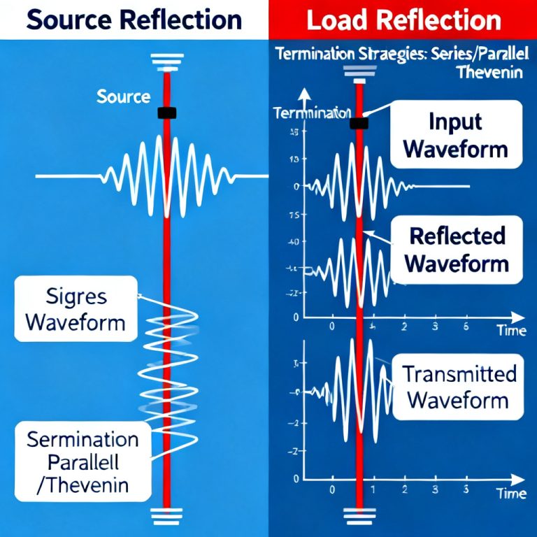
Blind & Buried Vias vs Through-Hole and Back Drilling
Engineers have three mainstream via solutions for multilayer high-speed projects: traditional through-hole vias, back drilling vias, and blind & buried vias. When evaluating blind buried via high speed pcb options, each differs greatly in routing density, signal performance, and manufacturing cost.
| Solution | Routing Density | High-Speed Signal Performance | Cost Level |
|---|---|---|---|
| Through-Hole Via | Low | Poor — long via stubs cause severe reflection, crosstalk and signal delay | Benchmark (Standard Cost) |
| Back Drilling Via | Medium | Good — removes most unused via stubs to optimize impedance stability | +10% – 20% vs benchmark |
| Blind & Buried Via | High | Excellent — completely eliminates via stubs, minimal parasitic interference | +25% – 50% vs benchmark |
Through-hole vias are only suitable for low-speed, low-density PCBs and not recommended for signals above 5GHz. Back drilling offers a cost-performance middle choice for mid-range high-speed boards with moderate density requirements. Blind buried via high speed pcb technology is the only reliable option for ultra-fine pitch BGA, miniaturized hardware, and high-frequency high-speed transmission systems.
For BGA fanout designs that often require blind vias, the BGA Fanout Techniques guide provides detailed layout recommendations for blind buried via high speed pcb implementations.
Common Application Scenarios for Blind and Buried Vias
Blind buried via high speed pcb technology is not required for every PCB project, but it becomes essential in the following high-demand scenarios:
Fine-Pitch BGA Layout
Mandatory for BGA fanout with pitch ≤ 0.8mm. Laser micro blind vias solve breakout routing limitations where traditional through-hole vias cannot fit dense pin arrays in blind buried via high speed pcb designs.
Ultra-High-Density Miniaturized Devices
Including smartphones, wearable electronics, medical endoscopes, compact industrial control modules, and portable detection equipment, where PCB size is strictly limited.
High-Speed & High-Frequency Hardware
Server motherboards, 5G base station boards, AI accelerator cards, radar systems, and high-speed communication devices that demand strict signal integrity, low loss, and stable impedance.
Complex Multilayer HDI PCBs
Boards with 6 layers or more that require efficient inner-layer power and signal interconnection without sacrificing outer routing space.
High-Speed Signal Integrity Benefits & Design Considerations
The biggest advantage of blind and buried vias in high-speed PCB design is complete stub elimination. Long via stubs in through-hole designs introduce extra parasitic inductance and capacitance, leading to signal reflection, timing skew, and increased insertion loss at high frequencies. Blind buried via high speed pcb technology eliminates these issues entirely.
With blind and buried vias, signal path length is minimized and kept consistent for differential pairs. Impedance control is more stable across the entire high-speed channel. Crosstalk between adjacent vias and traces is reduced significantly, supporting reliable signal transmission at 10Gbps+ high-speed interfaces. These are the core benefits of blind buried via high speed pcb design.
Designers should keep dielectric material Dk/Df parameters in mind, maintain consistent reference planes, and avoid placing high-speed vias close to board edges or gap areas to prevent EMI issues in blind buried via high speed pcb layouts.
Key Takeaways & Best Practices
- Blind and buried vias are foundational for modern HDI PCB and blind buried via high speed pcb design, enabling higher density, smaller size, and better signal integrity
- Select via type (1st-order, 2nd-order, stacked, staggered) based on layout density, BGA pitch, and budget to avoid over-designing unnecessary high-cost structures for your blind buried via high speed pcb project
- Always follow DFM rules parameter limits for aperture, pad size, dielectric thickness, and alignment tolerance to ensure manufacturing yield
- Confirm the PCB manufacturer’s capability in laser drilling, sequential lamination, and copper/resin via filling before finalizing your stackup and layout
- For cost-sensitive projects, use back drilling as an alternative; for high-speed, fine-pitch BGA and miniaturized products, prioritize blind buried via high speed pcb technology
Frequently Asked Questions (FAQ)
Q1: What is the main difference between blind via and buried via in blind buried via high speed pcb design?
A blind via connects outer layer to inner layer and is visible on one PCB surface; a buried via connects only inner layers and is completely hidden inside the board with no external exposure. This is a fundamental distinction in blind buried via high speed pcb design.
Q2: How much more expensive are blind and buried via PCBs for blind buried via high speed pcb projects?
Cost increases range from +15% up to +80%, depending on via order, stacked structure, layer count, and via filling requirements. Standard 1st-order blind vias only add 15–25% cost for blind buried via high speed pcb manufacturing.
Q3: What is the minimum aperture of a laser blind via in blind buried via high speed pcb?
Professional manufacturers can achieve 0.075mm minimum aperture for laser micro blind vias, suitable for 0.4mm fine-pitch BGA breakout in blind buried via high speed pcb designs.
Q4: Are blind and buried vias required for high-speed PCB?
Not mandatory for low-frequency designs, but strongly required for signals over 5GHz, fine-pitch BGA, and HDI miniaturized boards to maintain signal integrity. This is a key decision point in blind buried via high speed pcb planning.
Q5: What is the difference between stacked and staggered vias in blind buried via high speed pcb?
Stacked vias are vertically aligned for higher density but cost more and require higher precision. Staggered vias are offset, lower in cost, and reduce structural stress and lamination risk for blind buried via high speed pcb designs.
Custom PCB Design & Manufacturing Inquiry
If you are designing high-speed multilayer PCBs, HDI stackup layouts, or fine-pitch BGA fanout requiring blind buried via high speed pcb technology, our professional engineering team can provide one-stop technical service for your project.
We offer: Custom HDI stackup design • Blind buried via high speed pcb structure optimization • Full DFM manufacturability review • High-speed signal integrity consultation • Accurate PCB manufacturing quotation
Submit your Gerber files, layer stack requirements or BGA pitch specifications. Our team will deliver professional design suggestions, process feasibility analysis, and a competitive quote in the shortest time.
About HighSpeedPCBs.com
We are a specialized PCB design and manufacturing service provider serving industrial, automotive, medical, and communications OEMs worldwide. Our expertise in blind buried via high speed pcb design ensures your high-density and high-speed designs achieve optimal signal integrity. Complete manufacturing process documentation is available in the PCB Manufacturing & Testing Guidelines.
© 2026 HighSpeedPCBs.com — Professional High-Speed PCB Solutions