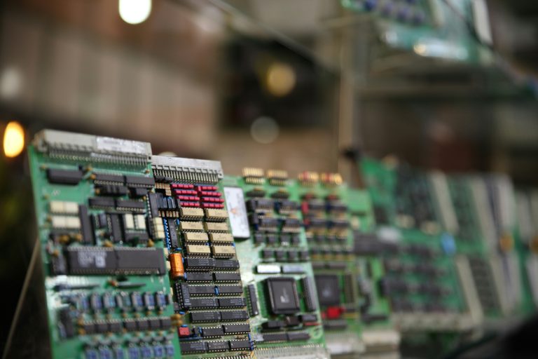
High speed PCB tolerance standards are the hidden core factor that determines signal integrity, yield and long-term reliability. As detailed in the High-Speed PCB Parameters master page, tolerance works together with impedance, copper thickness and Dk/Df values to determine final product performance. Theoretical design data never matches actual production output — minor deviations in impedance, trace width, layer alignment, drilling and board thickness can cause signal reflection, crosstalk, timing jitter and even circuit failure. This guide covers impedance tolerance grades, trace etching, layer registration, drilling, IPC classification, cost impact and design best practices for engineers and procurement buyers.
Why High Speed PCB Tolerance Standards Matter
In high-speed circuit design, there is a critical principle: the finished PCB never perfectly matches your design file. All simulation software assumes ideal conditions, but real PCB fabrication brings process deviations — these deviations are manufacturing tolerances. The High-Speed PCB Parameters master page provides a complete framework for understanding how high speed PCB tolerance standards interact with impedance, loss and material selection.
Tolerance directly controls signal integrity, impedance continuity and assembly compatibility. For 5G, server backplanes, optical modules and 112G PAM4 links, even small tolerance errors can trigger impedance discontinuity and severe jitter. There is an obvious trade-off: tighter tolerance = better performance + higher cost + longer lead time. Mastering high speed PCB tolerance standards allows you to make reasonable DFM rules at the early design stage.
Impedance High Speed PCB Tolerance Standards (Core Specification)
Controlled impedance is the foundation of high-speed signal transmission. Any fluctuation beyond the allowable range destroys differential pair matching. For a deeper understanding of how impedance is calculated, refer to Impedance Matching PCB. The industry divides impedance tolerance into three standardized grades:
| Grade | Impedance Tolerance | Typical Application | Cost Increase |
|---|---|---|---|
| Standard | ±10% | General high-speed PCB, below 25Gbps | Baseline |
| Strict | ±7% | High-end communication, 25G~56G links | +10%–20% |
| Precision | ±5% | 56G–112G PAM4 ultra-high-speed design | +25%–40% |
From IPC 2141 standard perspective, ±10% is the industrial baseline, while ±5% belongs to high-reliability precision control. Design best practice: Design high-speed traces based on ±10% first, then apply ±7% or ±5% only to critical differential pairs. Multiple factors affect impedance drift: dielectric constant deviation, copper thickness variation and trace width error. For material property data, refer to Dk/Df values high speed PCB. All these physical tolerances must be coordinated to stabilize high speed PCB tolerance standards.
Trace Width and Etching High Speed PCB Tolerance Standards
Trace width etching tolerance directly changes actual conductor width, a main cause of impedance deviation. Different copper weights have fixed etching tolerance ranges. For detailed guidance on copper weight, see copper thickness high speed PCB.
| Copper Weight | Nominal Trace Width | Etching Tolerance Range |
|---|---|---|
| 0.5oz | 4mil | ±0.5–0.8mil |
| 1oz | 5mil | ±0.8–1.0mil |
| 2oz | 8mil | ±1.0–1.5mil |
High-speed designers should avoid designing trace width at the process limit. Fine lines under 4mil should use 0.5oz thin copper to reduce relative etching deviation. If actual trace width shrinks beyond tolerance, impedance rises sharply and causes signal mismatch. Always confirm etching capability with your manufacturer before finalizing stackup.
Layer-to-Layer Registration High Speed PCB Tolerance Standards
Layer-to-layer registration means alignment accuracy between laminated inner layers, vital for HDI boards and blind/buried via design. Poor registration leads to via misalignment, increased crosstalk and even internal short circuits. Material stability plays a key role — high-performance laminates with stable Dk/Df help maintain alignment. See Dk/Df values high speed PCB for material guidance.
| Type | Registration Tolerance | Application Scenario |
|---|---|---|
| Standard | ±3mil | Conventional multilayer through-hole PCB |
| Advanced | ±2mil | Server, high-end communication PCB |
| HDI Precision | ±1–2mil | Laser blind via, sequential lamination HDI |
For 56G and above high-speed designs, do not use standard ±3mil registration. Sequential lamination technology achieves ±1~2mil ultra-precise registration. These high speed PCB tolerance standards are essential for dense via arrays and high-density routing.

Drilling Tolerances: Position, Aperture & Hole Wall Copper
Drilling tolerance includes three key indicators: hole position accuracy, aperture tolerance and plated hole wall copper thickness, all related to via impedance and thermal cycle performance.
| Parameter | Standard Process | Advanced High-Speed Process |
|---|---|---|
| Hole Position Accuracy | ±2mil | ±1mil |
| Aperture Dimension Tolerance | ±2mil | ±1mil |
| Avg Hole Wall Copper Thickness | ≥20μm | ≥25μm |
High-speed vias are sensitive to positional deviation. Dense via arrays for 56G/112G links must adopt ±1mil high-precision drilling. These high speed PCB tolerance standards ensure reliable via performance and soldering quality.
Board Thickness and Profile Outline Tolerances
Board thickness tolerance: Finished thickness ≤1.6mm: ±10% nominal thickness; >1.6mm: ±0.15mm fixed tolerance.
Profile outline tolerance: Standard routing/milling: ±0.2mm.
For high-precision pluggable interface boards, specify tighter outline tolerance, but this raises manufacturing cost. Always confirm board thickness tolerance with your factory early in design.
IPC Tolerance Classes 1 / 2 / 3 Full Explanation
IPC standard defines three reliability classes, the global benchmark for selecting high speed PCB tolerance standards.
IPC Class 1 – General Electronic Products: Loosest tolerance, for consumer electronics. Not suitable for any medium or high-speed signal design.
IPC Class 2 – Dedicated Service Electronic Products: Balanced tolerance, cost and reliability. Widely used in communication equipment, servers and industrial control boards. Fully meets 10G–56G high-speed PCB requirements.
IPC Class 3 – High-Reliability Electronic Products: Strictest tolerance, full testing required. Applied to medical, aerospace, automotive safety and core telecom. Mandatory for 112G PAM4 ultra-high-speed PCB.
Recommendation: All formal high-speed PCB projects adopt at minimum IPC Class 2; ultra-high-speed and high-reliability applications choose IPC Class 3.
How to Correctly Specify High Speed PCB Tolerance Standards by Application Speed
Prototype / Below 5Gbps: Standard tolerance (±10% impedance, ±3mil registration, standard drilling). Save cost for functional verification.
Mass Production / 10G–25Gbps: Standard tolerance for regular layers; tighten only critical differential pairs.
56G–112Gbps Ultra-High-Speed: ±7%~±5% impedance, ±1~2mil HDI registration, ±1mil drilling. For layout guidelines, refer to Differential Pair Routing Rules.
Core principle: Relax non-critical parameters, strictly control high-speed sensitive parameters. For complete guidance on all PCB parameters, return to the High-Speed PCB Parameters master page.
Key Takeaways & Design Principles
- ±10% impedance tolerance is the industry baseline; ±7% and ±5% for ultra-high-speed with higher cost.
- High speed PCB tolerance standards include etching, registration, drilling, board thickness and profile.
- Tighter tolerance = higher cost + longer lead time. Avoid over-specification.
- IPC Class 2 is mainstream for commercial high-speed PCB; Class 3 for medical, automotive and 112G.
- Confirm tolerance rules and process capability with your manufacturer at stackup design stage.
FAQ About High Speed PCB Tolerance Standards
Q1: What is the most common impedance tolerance for high-speed PCB?
±10% is universal for most commercial designs; ±7% for 25G~56G, ±5% for 112G PAM4 projects.
Q2: Does tighter layer registration affect signal quality?
Yes. Misaligned layers cause via offset and parasitic fluctuation, leading to jitter and crosstalk.
Q3: Can I mix standard and tight tolerances on one PCB?
Yes. Tighten only critical high-speed nets; keep other circuits at standard tolerance to control cost.
Q4: What IPC class for server and communication PCB?
IPC Class 2 is default; Class 3 for high reliability and long service life.
Q5: Does strict tolerance prolong lead time?
Yes. Precision tolerance adds 3–5 days lead time and 10%–40% cost.
Get Professional Tolerance Specification & PCB Quotation
Defining reasonable high speed PCB tolerance standards requires signal integrity experience and manufacturing knowledge. If you are designing 25G/56G optical modules, 112G PAM4 switches, server HDI boards or automotive PCBs, our engineering team provides one-on-one tolerance optimization and DFM evaluation.
Send your design files, stackup requirements and application scenario. We will customize the most suitable high speed PCB tolerance standards for you, balancing performance, cost and yield.
© 2026 HighSpeedPCBs