PCIe PCB design for 4.0/5.0/6.0: 100Ω impedance, intra-pair length matching (1-5mil), AC coupling caps (0402/0201), via limits (≤2), back-drilling, loss budget, and REFCLK routing. Includes version tables and layout checklist.
Introduction to PCIe PCB Design
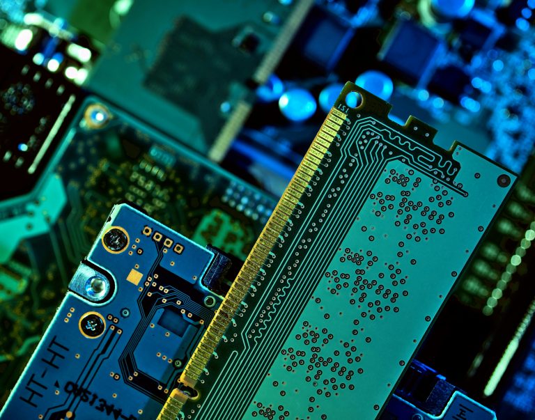
Peripheral Component Interconnect Express (PCIe) has become the mainstream high-speed serial bus standard for modern servers, data center storage, industrial PCs, AI embedded hardware, and consumer computing platforms. As detailed in the High-Speed Interfaces master page, PCIe is one of several critical protocols that demand specific layout rules. Unlike traditional parallel bus architectures, PCIe PCB design adopts point-to-point differential pair transmission, which places extremely high requirements on routing symmetry, impedance stability, and channel loss control.
Over the past decade, PCIe bandwidth has doubled with each new generation: PCIe 1.0 runs at 2.5 GT/s, evolving to PCIe 5.0 with 32 GT/s using NRZ signaling. The latest PCIe 6.0 upgrades to 64 GT/s with PAM4 modulation, further doubling transmission speed while bringing stricter challenges in signal integrity, material loss, and routing constraints.
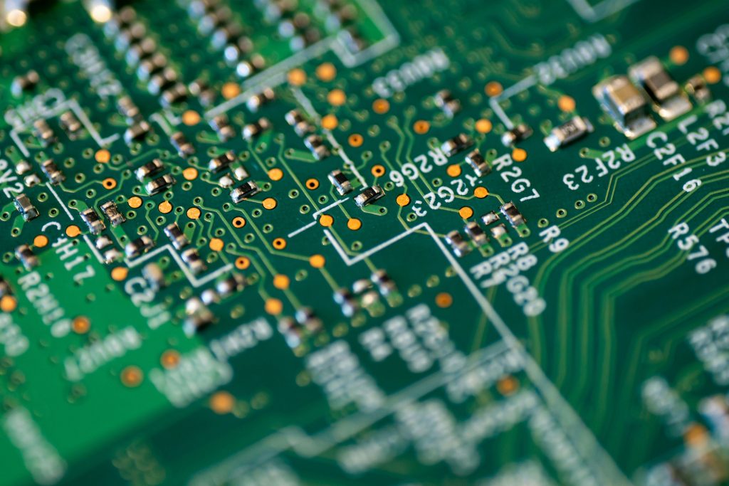
High-speed PCIe PCB design requires systematic control of dielectric loss, copper foil roughness, trace impedance, length skew, crosstalk, via stub loss, and reference plane continuity. This guide integrates official specifications from industry standards to help engineers achieve mass-production-ready PCIe 4.0, 5.0, and 6.0 implementation.
PCIe Generations and PCIe PCB Design Loss Budget
Each PCIe generation has independent data rate, encoding scheme, and maximum allowable insertion loss budget. Understanding Insertion Loss is critical because PCIe 6.0 PAM4 modulation is more sensitive to noise and jitter than NRZ.
| Generation | Data Rate | Encoding / Modulation | Max Insertion Loss |
|---|---|---|---|
| PCIe 3.0 | 8 GT/s | 128b/130b NRZ | <25dB |
| PCIe 4.0 | 16 GT/s | 128b/130b NRZ | <28dB |
| PCIe 5.0 | 32 GT/s | 128b/130b NRZ | <36dB |
| PCIe 6.0 | 64 GT/s | PAM4 | <40dB |
Proper PCIe PCB design must allocate loss budget across PCB traces, connectors, vias, and AC coupling capacitors to meet these targets.
PCB Material Selection for PCIe PCB Design
PCB substrate material is the foundation of high-speed PCIe layout. Lower Df (dissipation factor) means lower signal transmission loss. For detailed Dk/Df values, refer to High-Speed PCB Material.
- PCIe 3.0 / 4.0: Standard FR4 acceptable; low-loss laminates recommended for long channels.
- PCIe 5.0: Low-loss laminate with low Df is mandatory for PCIe PCB design at 32 GT/s.
- PCIe 6.0: Ultra-low-loss laminate required, with strict copper foil roughness control.
Differential Impedance and Length Matching in PCIe PCB Design
All PCIe TX/RX lanes adopt 100Ω differential impedance across all generations, with ±10% tolerance. The foundational rules for Differential Pair Routing apply directly to PCIe layout.
| Design Rule | PCIe 4.0 | PCIe 5.0 | PCIe 6.0 |
|---|---|---|---|
| Differential Impedance | 100Ω ±10% | 100Ω ±10% | 100Ω ±10% |
| Intra-pair Length Mismatch | ≤5 mil | ≤2–3 mil | ≤1–2 mil |
| Inter-pair Lane Mismatch | ≤8 mil | ≤5 mil | ≤3–5 mil |
| Max Vias Per Signal Pair | ≤2 | ≤2 | ≤2 |
For PCIe 5.0/6.0, excessive intra-pair skew causes timing offset and link training failure. When using serpentine routing for compensation, keep height ≤ 3× trace width and spacing ≥ 4× trace width to avoid crosstalk. These are essential PCIe PCB design rules for high-speed success.
AC Coupling Capacitor Placement in PCIe PCB Design
PCIe specifications mandate AC coupling capacitors on each transmit lane.
Placement: Place capacitors close to TX side. Differential traces must maintain symmetry through the capacitor.
Package Selection: PCIe 4.0: 0402 acceptable. PCIe 5.0/6.0: 0201 mandatory to reduce parasitic capacitance.
Optimization: Remove ground reference plane under capacitor pads (anti-pad) to improve signal integrity.
PCIe Reference Clock (REFCLK) Routing for PCIe PCB Design
All PCIe lanes synchronize to a 100MHz differential reference clock.
Core rules: 100Ω differential pair; intra-pair mismatch ≤2 mil (stricter than data lines); ground guard vias on both sides for shielding; keep away from TX/RX lanes; continuous ground reference plane underneath.
For PCIe 5.0/6.0, use inner-layer stripline routing for optimal shielding.
Via Limits, Anti-Pad and Back-Drilling in PCIe PCB Design
Maximum 2 vias per TX/RX differential pair. Back-drilling is strongly recommended for PCIe 5.0/6.0 to remove via stub reflections. Use ground return vias around signal vias to suppress crosstalk.
Stackup and Reference Plane Principles
Never route PCIe differential pairs across split ground or power planes. Split planes destroy the return path and cause impedance mutation. Use symmetric multilayer stackup with stripline routing on inner layers for better shielding.
Complete PCIe PCB Design Layout Checklist
| Item | Requirement |
|---|---|
| ✅ Differential impedance | 100Ω ±10% on all TX/RX pairs |
| ✅ Intra-pair length matching | Per generation table |
| ✅ Inter-pair lane matching | Per generation table |
| ✅ AC coupling capacitors | 0402 (Gen4) or 0201 (Gen5/6) |
| ✅ Max vias per signal | ≤2 |
| ✅ Back-drilling | Required for Gen5/6 |
| ✅ Reference plane | No splits under PCIe traces |
| ✅ REFCLK routing | 100Ω, intra-pair ≤2mil, guarded |
Key Takeaways for PCIe PCB Design
- PCIe 6.0 intra-pair skew must be ≤1-2 mil
- 100Ω differential impedance is standard across all generations
- AC coupling requires 0201 package for Gen5/6
- Back-drilling is mandatory for Gen5/6
- Never route PCIe traces across split planes
- Low-loss materials are required for Gen5/6 PCIe PCB design
Frequently Asked Questions About PCIe PCB design
Q1: Can I use standard FR4 for PCIe 5.0?
No. Standard FR4 has high Df loss. Low-loss laminates are required.
Q2: Why is intra-pair matching so strict for PCIe 6.0?
PCIe 6.0 uses PAM4 with smaller eye opening, extremely sensitive to timing skew.
Q3: Is back-drilling necessary for PCIe 5.0?
Highly recommended and almost mandatory for mass production.
Q4: Where to place PCIe AC coupling capacitors?
Priority near TX end, with symmetric routing and anti-pad design.
Q5: What is the standard PCIe differential impedance?
100Ω ±10% for all generations.
Get Professional PCIe PCB Design Review
Need help with PCIe 4.0, 5.0, or 6.0 layout? Our team provides stackup validation, impedance calculation, loss budget analysis, layout rule checking, and DFM review. Send your design files for a free professional evaluation and quotation.
© 2026 HighSpeedPCBs