Ethernet PCB design covers all critical design rules for 10G, 25G, and 100G backplane and interface routing for industrial, data center, and telecom hardware. It integrates industry-standard specifications, differential impedance control, length matching tolerances, backplane design challenges, connector layout rules, Ethernet magnetics placement, and a complete layout checklist.
Compiled based on official technical guidelines from Cadence, TI, and Samtec, this article balances professional signal integrity depth with easy-to-understand explanations for hardware engineers, PCB designers, procurement specialists, and industrial buyers. You will learn clear comparison tables, parameter benchmarks, practical layout solutions, and common pitfalls to avoid in high-speed Ethernet PCB design.
Overview of Ethernet PCB Design
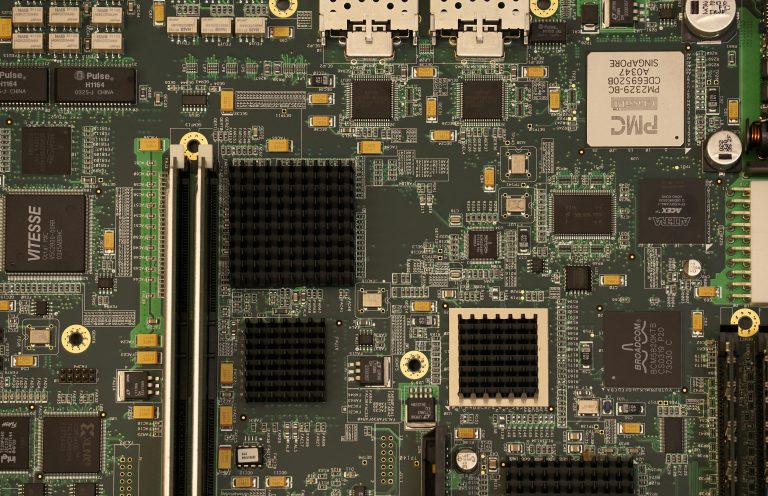
Ethernet remains the dominant communication standard for local area networks, industrial equipment, rack-mounted chassis, and data center backplane interconnection. As detailed in the High-Speed Interfaces master page, Ethernet is one of several critical protocols that demand specific layout rules alongside PCIe, DDR, and USB. From legacy 10Mbps traditional Ethernet to modern high-speed SerDes architectures supporting up to 112G per lane, Ethernet has evolved to meet explosive bandwidth demands in server, telecom, and industrial control systems.
Compared with ordinary onboard signal routing, Ethernet backplane Ethernet PCB design brings far stricter signal integrity challenges: longer channel transmission distance, multi-layer stackup limitations, connector impedance discontinuity, via stub resonance, crosstalk interference, and accumulated insertion loss.
A well-designed high-speed Ethernet PCB must follow standardized routing rules, precise impedance control, reasonable material selection, and complete reference plane design. This guide consolidates industry best practices from top EDA vendors, semiconductor manufacturers, and high-speed connector leaders, providing a one-stop reference for 10G, 25G, and 100G Ethernet layout.
Ethernet Standards for Ethernet PCB Design
Before starting PCB layout, designers must clarify the corresponding Ethernet standard, as each protocol defines data rate, per-lane SerDes speed, encoding scheme, and application scenarios — all of which directly determine PCB stackup, material grade, routing density, and loss budget planning.
Below is the authoritative comparison table for mainstream Ethernet standards used in PCB design:
| Standard | Aggregate Rate | Per Channel Rate | Encoding | Typical Application |
|---|---|---|---|---|
| 1000BASE-T | 1 Gbps | 125 MHz | PAM5 | Onboard routing, RJ45 copper port |
| 10GBASE-KR | 10.3125 Gbps | 10.3125G | 64b/66b | Server & chassis backplane |
| 25GBASE-KR | 25.78125 Gbps | 25.78G | 64b/66b | High-density data center backplane |
| 100GBASE-KR4 | 100 Gbps | 4×25.78G | 64b/66b | 4-lane parallel backplane interconnection |
| 100GBASE-KP4 | 100 Gbps | 4×25.78G PAM4 | 64b/66b | PAM4 modulation low-latency backplane |
Legacy 1000BASE-T uses PAM5 modulation with low frequency requirements, allowing standard FR4 material and relaxed routing rules. 10G/25GBASE-KR adopt 64b/66b encoding to balance transmission efficiency and DC balance. 100GBASE-KP4 applies PAM4 modulation to double bandwidth within the same physical lanes, which imposes higher requirements on PCB loss performance and impedance stability.
As single-lane speed exceeds 10Gbps, ordinary FR4 cannot meet high-frequency loss demands, and low-loss dielectric materials plus HVLP copper foil become essential for stable link operation. For detailed material selection guidance, refer to High-Speed PCB Material.
Differential Impedance & Length Matching Requirements
Impedance control and length matching are the two foundational rules of high-speed Ethernet PCB design. Uncontrolled impedance causes signal reflection; excessive length mismatch leads to timing skew, common-mode noise, and link training failure.
All 10G to 100G Ethernet differential pairs adopt a unified 100Ω differential impedance standard, while tolerance and length matching rules become tighter as speed increases.
| Parameter | 10G Ethernet | 25G Ethernet | 100G Ethernet |
|---|---|---|---|
| Differential Impedance | 100Ω ±10% | 100Ω ±10% | 100Ω ±10% |
| Intra-Pair Length Mismatch | ≤5 mil | ≤3 mil | ≤2–3 mil |
| Inter-Pair Length Mismatch | ≤10 mil | ≤5 mil | ≤5 mil |
| Channel Insertion Loss Budget | <30dB | <30dB | Follow IC vendor specs |
Key Design Notes:
- Calculate 100Ω differential impedance strictly based on stackup, dielectric constant, trace width, and layer thickness; keep manufacturing tolerance within ±10%.
- Intra-pair length matching ensures synchronous signal edge arrival to suppress EMI and common-mode noise.
- Inter-pair length matching synchronizes multi-lane parallel channels to avoid lane skew in KR4 architectures.
- For 100G designs, do not follow general loss standards blindly; always comply with the transceiver chip vendor’s official loss budget curve, including traces, vias, connectors, and backplane channels.
The foundational rules for Differential Pair Routing apply directly to Ethernet layout, covering length matching, gap control, and tight coupling.
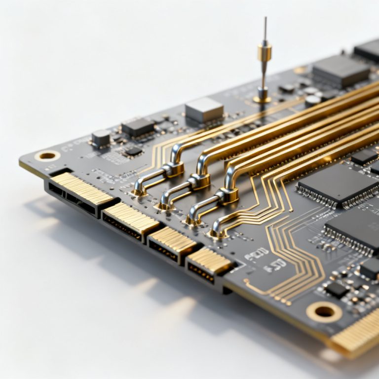
High-Speed Backplane Design Guidelines & Solutions
Ethernet backplane design is the most difficult part of high-speed layout, facing long-channel loss, connector discontinuity, via stubs, crosstalk, and discontinuous return current paths. Understanding Insertion Loss is critical for backplane design, as longer channels accumulate more attenuation.
Below is the industry-standard challenge-to-solution framework adopted by Cadence, Samtec and TI:
| Core Challenge | Professional Design Solution |
|---|---|
| Long channel high insertion loss | Adopt low-loss high-frequency PCB dielectric material + HVLP low-roughness copper foil to reduce skin effect and dielectric loss |
| Connector pin impedance discontinuity | Select high-speed optimized backplane connectors; strictly follow vendor pin assignment and fanout guidelines |
| Via stub resonance & extra loss | Apply back drilling process to remove unused stub segments of high-speed signal vias |
| Inter-pair crosstalk | Increase differential pair spacing, add ground stitching vias between channels, and apply 3W/5W routing rules |
| Discontinuous return current path | Maintain complete, unbroken ground reference plane; add dense stitching vias at layer transitions and routing boundaries |
For 25G and 100G backplane applications, standard FR4 is no longer sufficient. Designers must select high-grade low-loss materials such as Megtron series or equivalent high-frequency substrates. Back drilling is not an optional process but a must for mass production to guarantee low bit error rate and stable long-term operation. For detailed manufacturing guidelines on via placement, back drilling, and stackup, refer to PCB Manufacturing.
Ethernet Connector Layout Best Practices
Ethernet connector layout determines routing starting points, impedance continuity, and signal path integrity. Three mainstream types include RJ45 copper connectors, SFP/QSFP optical module connectors, and high-speed backplane connectors.
RJ45 Copper Connector
- Route differential pairs closely from connector pins to minimize stub length.
- Keep consistent trace width and spacing; avoid immediate layer switching right after pin fanout.
- Isolate high-speed Ethernet traces away from clock lines, power routes, and low-speed control signals to reduce crosstalk.
SFP / QSFP Optical Module Connector
- Follow official high-speed layout specifications for cage grounding, keep-out zone definition, and differential fanout routing.
- Reserve thermal pad grounding design and complete surrounding ground stitching for heat dissipation and EMI suppression.
High-Speed Backplane Connector
- Strictly implement the manufacturer’s layout guide, pin grouping, fanout via placement, and keep-out zone requirements.
- Do not modify pin assignment arbitrarily; vendor pin fields are pre-optimized for impedance matching and crosstalk isolation.
Ethernet Magnetics and Common Mode Choke Layout Rules
Ethernet transformers and common mode chokes are critical for isolation, common-mode noise suppression, surge protection, and EMC performance in RJ45-based Ethernet circuits.
Core layout rules:
- Place magnetics components as close to RJ45 as possible to shorten unprotected trace length and avoid external noise coupling.
- Keep differential routing completely symmetrical through transformers and chokes to avoid extra intra-pair skew.
- Hollow out ground and power planes directly beneath magnetics to eliminate parasitic capacitance, prevent impedance discontinuity and high-frequency resonance.
- Separate analog and digital ground properly, follow center tap grounding rules, and match recommended resistance networks for better surge and EMC performance.
Proper magnetics placement is a key factor in successful Ethernet PCB design for industrial and telecom applications with stringent EMC requirements.
Complete Ethernet PCB Layout Checklist
Use this checklist to verify your 10G/25G/100G Ethernet design before finalizing layout and manufacturing:
| ✅ | Item |
|---|---|
| ✅ | Confirm all differential pairs maintain 100Ω impedance within ±10% tolerance |
| ✅ | Check intra-pair and inter-pair length mismatch fully complies with 10G/25G/100G mil limits |
| ✅ | Apply back drilling for all high-speed signal vias to eliminate residual stubs |
| ✅ | Ensure full and uninterrupted ground reference planes for all Ethernet high-speed traces |
| ✅ | Follow official layout guidelines for RJ45, SFP/QSFP and backplane connectors |
| ✅ | Ethernet magnetics placed near RJ45 with symmetric routing and plane hollowing underneath |
| ✅ | Verify channel insertion loss is within budget; select low-loss material for 25G+ backplane design |
| ✅ | Add sufficient ground stitching vias to suppress crosstalk and stabilize return current paths |
Key Takeaways
- 10G to 100G Ethernet PCB design is a systematic project combining protocol standards, signal integrity, PCB material performance, and manufacturing processes.
- 25G and 100G backplane designs require low-loss dielectric material + HVLP copper foil as standard configuration.
- Back drilling is mandatory to solve via stub resonance and high-frequency loss issues.
- The biggest pain points of backplane design are connector impedance discontinuity, long-channel insertion loss, and inter-pair crosstalk.
- Insertion loss budget should be confirmed first to guide stackup layer count, material selection, and copper foil specification.
- Strictly following impedance control, length matching, reference plane integrity, and vendor connector rules can avoid most SI and EMC problems.
For a complete understanding of all high-speed interface layout requirements, return to the High-Speed Interfaces master page.
FAQ About 10G/25G/100G Ethernet PCB Design
Q1: What is the standard differential impedance for Ethernet high-speed lines?
All mainstream 10G/25G/100G Ethernet differential pairs use 100Ω differential impedance, with typical tolerance ±10%.
Q2: Is back drilling necessary for 25G and 100G Ethernet backplane?
Yes. Without back drilling, via stubs will cause serious resonance and insertion loss, leading to unstable link and high bit error rate.
Q3: What length matching tolerance should I follow for 100G Ethernet?
Intra-pair length mismatch controlled within 2–3 mil, inter-pair no more than 5 mil.
Q4: Why hollow out the plane under Ethernet transformers?
To eliminate parasitic capacitance between component pins and reference planes, avoid impedance mutation and improve EMC performance.
Q5: Can regular FR4 be used for 25G and 100G backplane design?
No. Ordinary FR4 has excessive high-frequency dielectric loss; low-loss specialized high-speed PCB material is required for Ethernet PCB design above 10G.
Professional Ethernet PCB Design Review & Consulting
Designing 10G, 25G, 100G Ethernet interface and backplane PCB requires rich signal integrity experience, stackup optimization, impedance simulation, and manufacturing process coordination. Minor layout non-compliance may result in unstable network links, high error rates, EMC failure, or low production yield.
If you need professional Ethernet PCB layout review, SI/PI simulation, stackup design, layout optimization, or project technical consulting and quotation support, our engineering team can provide one-stop high-speed interface design services.
Leave your project requirements via our inquiry page, and we will arrange a professional engineer to communicate with you, offer technical suggestions and customized solution quotes according to your 10G/25G/100G Ethernet application scenario.
© 2026 HighSpeedPCBs –