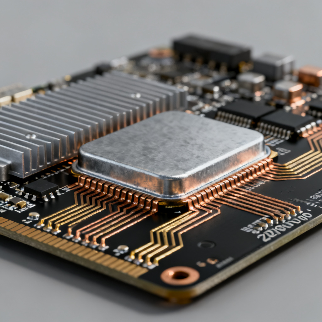
In the world of High Speed PCB Design, mastering key terminology is critical for achieving signal integrity, minimizing electromagnetic interference, and ensuring reliable performance at high frequencies. This glossary consolidates the most authoritative insights from leading industry resources, covering everything from basic concepts to advanced design techniques for your custom PCB production needs.
Whether you are a design engineer, procurement specialist, or manufacturer, these 50 terms will empower you to communicate effectively, optimize designs, and avoid costly errors in high speed PCB manufacturing.
Core Concepts and Fundamentals of High Speed PCB Design
1. Signal Integrity (SI)
Signal Integrity refers to the quality of an electrical signal as it travels through a PCB trace. In High Speed PCB Design, maintaining SI is paramount to prevent distortion, reflections, and timing errors. Factors like impedance mismatches, crosstalk, and dielectric losses degrade SI. Practical steps include controlled impedance routing, minimizing stub lengths, and using proper termination techniques.
2. Impedance
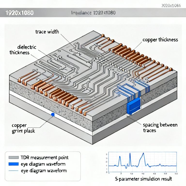
Impedance is the opposition to the flow of alternating current (AC) in a circuit, measured in ohms (Ω). For high-speed PCBs, controlled impedance (e.g., 50Ω single-ended, 100Ω differential) is essential to match the characteristic impedance of transmission lines, preventing signal reflections. Key variables include trace width, thickness, dielectric constant (Dk), and distance to reference planes.
3. Transmission Line
A transmission line is a conductive path (e.g., a PCB trace) designed to carry high-frequency signals with minimal loss. It consists of a signal conductor and a return path (usually a ground plane). Common types include microstrip and stripline. Proper transmission line design ensures signal integrity over long distances.
4. Microstrip
A microstrip is a type of transmission line where the signal trace is on the outer layer of the PCB, separated from a reference plane (ground or power) by a dielectric material. It offers easier access for components but is more susceptible to EMI and radiation. Impedance is controlled by trace width, dielectric thickness, and Dk.
5. Stripline
A stripline is a transmission line embedded between two reference planes (e.g., ground layers) within the PCB stackup. It provides superior isolation and reduced EMI compared to microstrip, making it ideal for high-speed, noise-sensitive signals. However, it requires more layers and is harder to route.
6. Dielectric Constant (Dk or Er)
The dielectric constant is a material property that measures how much an electric field is reduced within the insulating material (substrate) compared to vacuum. In High Speed PCB Design, low and stable Dk (e.g., 3.0–4.5 for FR4, lower for Rogers materials) minimizes signal delay and loss. Variations in Dk can cause impedance inconsistencies.
7. Dissipation Factor (Df)
Also known as loss tangent, Df quantifies the energy lost as heat in the dielectric material when an AC signal passes through. Low Df (e.g., <0.005 for high-speed laminates) is critical for reducing signal attenuation at high frequencies. Materials like PTFE (Teflon) or ceramic-filled laminates offer low Df.
8. Skin Effect
Skin effect is the tendency of high-frequency AC current to concentrate near the surface of a conductor, reducing its effective cross-sectional area and increasing resistance. At frequencies above 1 GHz, this effect becomes significant, leading to higher ohmic losses. Mitigation strategies include using wider traces, thicker copper (e.g., 2 oz), or surface finishes like ENIG.
9. Propagation Delay
Propagation delay is the time it takes for a signal to travel from the transmitter to the receiver, typically measured in nanoseconds per inch (ns/in). For high-speed designs, managing propagation delays is vital to meet timing constraints. It depends on the dielectric constant and trace length. Typical values: 150–200 ps/in for FR4.
10. Rise Time and Fall Time
Rise time (Tr) is the time a signal takes to transition from 10% to 90% of its final voltage, while fall time (Tf) is the reverse. Faster rise/fall times (e.g., <1 ns) indicate higher frequency content, increasing the risk of reflections and EMI. Designers must account for these to maintain signal quality.
Design and Routing Techniques for High Speed PCB
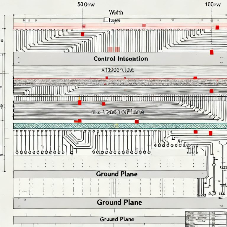
11. Controlled Impedance
Controlled impedance is the deliberate design of PCB traces to achieve a specific characteristic impedance (e.g., 50Ω ±10%). This is achieved by adjusting trace geometry (width, spacing) and stackup parameters (dielectric thickness, Dk). It is mandatory for high-speed signals like DDR, PCIe, and USB.
12. Differential Pair
A differential pair consists of two traces carrying complementary signals (e.g., + and -). The impedance is defined as the differential impedance (e.g., 100Ω). Key parameters include trace width, spacing (gap), and length matching. Differential signaling offers better noise immunity and lower EMI.
13. Length Matching
Length matching ensures that multiple traces in a bus (e.g., data lines in DDR memory) have equal electrical lengths to minimize skew—the timing difference between signals arriving at the destination. Techniques include serpentine routing, trombone shapes, or adding meanders. Tolerance is often within ±10 mils.
14. Skew
Skew is the difference in propagation delay between signals in a group (e.g., clock and data lines). Excessive skew can cause setup/hold time violations. Length matching and careful routing of differential pairs help control skew.
15. Crosstalk
Crosstalk is the unwanted coupling of energy between adjacent traces, caused by capacitive or inductive interference. It can lead to signal corruption. Mitigation techniques include increasing trace spacing (3W rule—3 times trace width), using guard traces, and routing perpendicularly on adjacent layers.
16. Guard Trace
A guard trace is a grounded trace placed between two signal traces to reduce crosstalk. It acts as a shield, absorbing electromagnetic fields. For high-speed designs, guard traces are often used with vias to ground planes at regular intervals (e.g., every λ/10).
17. Return Path
The return path is the route taken by current returning to its source via the ground or power plane. In High Speed PCB Design, a continuous, low-inductance return path is critical. Discontinuities (e.g., slots in ground planes) cause signal integrity issues like increased EMI and impedance mismatches.
18. Via
A via is a plated hole used to connect traces between different layers of a PCB. In high-speed designs, vias introduce parasitic inductance and capacitance. To minimize effects, use microvias, back-drilling, or via stitching. Avoid stub vias (unused portions) that cause reflections.
19. Back Drilling
Back drilling is the process of removing the unused portion of a through-hole via (the stub) that extends beyond the target layer. This reduces signal reflections and improves signal integrity, especially for high-speed signals above 1 GHz.
20. Via Stitching
Via stitching involves placing multiple vias along ground planes or around high-speed traces to create a low-impedance path and reduce EMI. It is commonly used in RF and high-speed digital designs.
21. Fan-Out
Fan-out refers to the routing of signals from a fine-pitch component (e.g., BGA) to larger pads or vias for easier routing. In high-speed designs, fan-out must maintain impedance control and minimize stub lengths.
22. Serpentine Routing
Serpentine routing uses meandering traces to adjust signal lengths for timing matching. It is common in DDR memory buses. However, excessive serpentine can increase crosstalk and signal loss, so it should be used sparingly.
23. Trombone Routing
Trombone routing is a length-matching technique using U-shaped bends, similar to a trombone slide. It offers more controlled impedance than sharp 90-degree bends and is preferred for high-speed signals.
24. 45-Degree Bend
Using 45-degree angled bends instead of 90-degree corners reduces impedance discontinuities and reflections. This is a standard practice in High Speed PCB Design.
Materials and Stackup for High Speed PCB
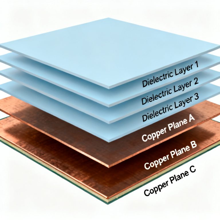
25. Stackup
Stackup is the arrangement of copper layers and dielectric materials in a PCB. For high-speed designs, a proper stackup (e.g., 4-layer, 8-layer) ensures controlled impedance, signal isolation, and power integrity. Common configurations include signal-ground-power-signal.
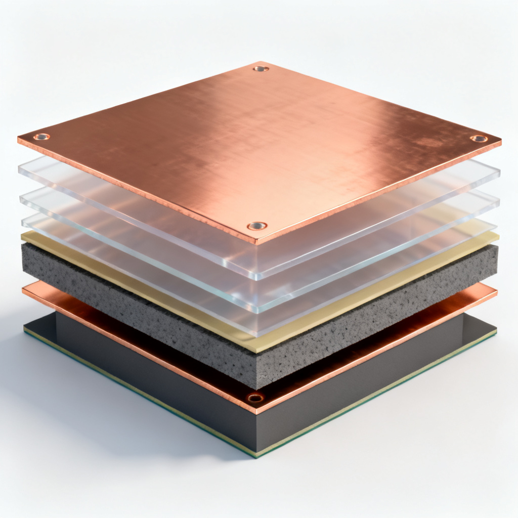
26. Prepreg
Prepreg is a partially cured fiberglass sheet impregnated with resin, used as a bonding layer between copper layers in multilayer PCBs. Its dielectric properties (Dk, Df) affect impedance and signal loss. Low-loss prepregs (e.g., 370HR) are used for high-speed designs.
27. Core
Core is a fully cured fiberglass sheet with copper foil on both sides, forming the base layer of a PCB. In high-speed designs, cores with low Dk and Df (e.g., Rogers 4350B) are preferred.
28. Low-Loss Laminates
Low-loss laminates (e.g., Rogers RO4000 series, Isola IS420) are materials with low Dk and Df, designed for high-frequency applications. They reduce signal attenuation and are essential for RF, microwave, and high-speed digital circuits.
29. Copper Weight
Copper weight (e.g., 1 oz, 2 oz) refers to the thickness of copper foil per square foot. Heavier copper (e.g., 2 oz) reduces resistance and skin effect losses in high-speed traces but increases manufacturing complexity.
30. Surface Finish
Surface finish protects exposed copper pads from oxidation. For high-speed designs, finishes like ENIG (Electroless Nickel Immersion Gold) or immersion silver offer low loss and good solderability, while HASL (Hot Air Solder Leveling) is less suitable due to uneven surfaces.
Signal Integrity and Analysis in High Speed PCB Design
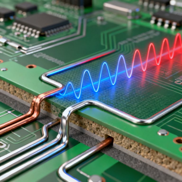
31. Reflection
Reflection occurs when a signal encounters an impedance mismatch (e.g., at a via, connector, or trace end), causing part of the signal to bounce back. This can lead to overshoot, undershoot, and ringing. Termination techniques (series, parallel, AC) mitigate reflections.
32. Termination
Termination is the addition of resistors or other components at the end of a transmission line to match impedance and absorb reflected energy. Common types include series termination (e.g., 33Ω resistor near driver), parallel termination (e.g., 50Ω to ground), and AC termination (capacitor in series).
33. Overshoot and Undershoot
Overshoot is when a signal exceeds its target voltage (e.g., above VCC), while undershoot is below ground. Both can damage components or cause logic errors. Proper impedance matching and termination reduce these phenomena.
34. Ringing
Ringing is the oscillation of a signal after a transition (e.g., a damped sine wave). It is caused by reflections and parasitic inductance/capacitance. Ringing can be minimized with termination and controlled impedance.
35. Eye Diagram
An eye diagram is a graphical representation of a digital signal’s quality, created by overlaying multiple bit transitions. A wide, open eye indicates good signal integrity, while a closed eye suggests noise, jitter, or timing issues. It is a key tool for validating high-speed designs.
36. Jitter
Jitter is the deviation of a signal’s timing from its ideal position, measured in picoseconds (ps). It can be random (e.g., thermal noise) or deterministic (e.g., crosstalk). Jitter degrades timing margins and is critical in high-speed serial interfaces (e.g., PCIe, USB).
37. Bit Error Rate (BER)
BER is the ratio of erroneous bits to total bits transmitted. In high-speed designs, a low BER (e.g., <10^-12) is required for reliable data transmission. Signal integrity issues like jitter and crosstalk increase BER.
38. Time Domain Reflectometry (TDR)
TDR is a measurement technique that sends a pulse down a transmission line and analyzes reflections to determine impedance discontinuities. It is used to validate impedance control and identify faults in high-speed PCBs.
39. S-Parameters
S-parameters (scattering parameters) describe the electrical behavior of a network (e.g., a PCB trace) at high frequencies. They measure signal reflection (S11), transmission (S21), and coupling (S31). S-parameters are essential for simulating high-speed designs.
40. Insertion Loss
Insertion loss is the reduction in signal power as it travels through a transmission line, measured in dB. It is caused by conductor losses (skin effect) and dielectric losses (Df). Low insertion loss is critical for high-speed signals over long traces.
41. Return Loss
Return loss is the ratio of reflected power to incident power, measured in dB. High return loss (e.g., >20 dB) indicates good impedance matching, while low return loss suggests reflections. It is a key parameter for high-speed interfaces.
Power Integrity and EMI in High Speed PCB
42. Power Integrity (PI)
Power integrity refers to the stability of power and ground voltages across a PCB. In High Speed PCB Design, PI is critical to prevent voltage droops, noise coupling, and timing errors. Techniques include using decoupling capacitors, power planes, and low-inductance paths.
43. Decoupling Capacitor
A decoupling capacitor is a capacitor placed near a power pin to filter high-frequency noise and provide local charge storage. For high-speed designs, use multiple capacitors with different values (e.g., 0.1 µF, 0.01 µF) and low equivalent series inductance (ESL).
44. Power Plane
A power plane is a continuous copper layer dedicated to a voltage (e.g., VCC). It provides a low-impedance power distribution network (PDN) and acts as a reference plane for return currents. In high-speed designs, power planes should be solid (no splits) to maintain signal integrity.
45. Ground Plane
A ground plane is a continuous copper layer dedicated to ground. It provides a stable reference for signals, reduces EMI, and supports return currents. Always use a solid ground plane under high-speed traces.
46. Electromagnetic Interference (EMI)
EMI is unwanted electromagnetic radiation from a PCB that can interfere with other devices. High-speed signals are common sources of EMI. Mitigation includes shielding, ground planes, filtering, and proper routing (e.g., avoiding long parallel traces).
47. Electromagnetic Compatibility (EMC)
EMC is the ability of a device to operate without causing or being affected by EMI. High-speed PCB designs must comply with EMC standards (e.g., FCC, CE). Techniques include filtering, grounding, and layout optimization.
48. Shielding
Shielding involves enclosing a circuit or trace in a conductive material (e.g., a metal can or ground plane) to block EMI. In PCBs, shielding can be achieved with guard traces, ground planes, or dedicated shields.
Advanced and Specialized Terms in High Speed PCB Design
49. Blind Via and Buried Via
Blind via connects an outer layer to an inner layer without going through the entire board. Buried via connects two inner layers without reaching the outer layers. Both reduce stub lengths and improve signal integrity in high-density, high-speed designs.
50. Microvia
A microvia is a small via (typically < 0.006″ diameter) used in high-density interconnect (HDI) PCBs. It supports fine-pitch components and reduces parasitic effects. Microvias are essential for high-speed designs with limited space.
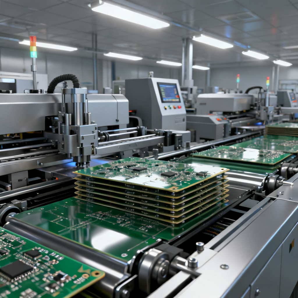
Why Choose Our High Speed PCB Manufacturing Services
We specialize in custom High Speed PCB production with advanced capabilities including controlled impedance, back drilling, low-loss laminates, and precise length matching. Unlike generic PCB manufacturers, we offer dedicated engineering support to ensure your design meets strict signal integrity and power integrity standards. Our stackup options include 4-layer to 20-layer configurations with materials like Rogers RO4000 and Isola IS420, providing low Dk and Df for GHz-frequency applications.
| Parameter | Our High Speed PCB Capability | Standard Industry Capability |
|---|---|---|
| Controlled Impedance Tolerance | ±5% | ±10% |
| Minimum Trace Width/Spacing | 3 mil / 3 mil | 4 mil / 4 mil |
| Back Drilling Depth Accuracy | ±2 mil | ±5 mil |
| Low-Loss Laminate Options | Rogers, Isola, Taconic | FR4 only |
| Surface Finish for High Speed | ENIG, Immersion Silver | HASL |
Frequently Asked Questions About High Speed PCB Design
What is the most important factor in High Speed PCB Design?
The most critical factor in High Speed PCB Design is maintaining signal integrity through controlled impedance, proper stackup, and minimizing reflections and crosstalk. Without these, high-frequency signals degrade rapidly.
How do I choose materials for High Speed PCB?
For High Speed PCB Design, select low-loss laminates with low Dk and Df, such as Rogers RO4000 or Isola IS420. Match the material to your operating frequency and budget. FR4 is suitable only for lower frequencies below 1 GHz.
What is the difference between microstrip and stripline in High Speed PCB?
In High Speed PCB Design, microstrip is on the outer layer and easier to route but more prone to EMI. Stripline is embedded between planes, offering better isolation and lower radiation, ideal for sensitive signals.
Can you manufacture High Speed PCBs with controlled impedance?
Yes, we specialize in manufacturing High Speed PCBs with controlled impedance tolerances as tight as ±5%, using advanced stackup and testing methods like TDR to ensure compliance.
Conclusion and Call to Action
Mastering these 50 High Speed PCB Design Terminology terms is your first step toward creating reliable, high-performance designs. At [Your Company Name], we specialize in manufacturing custom High Speed PCBs with advanced capabilities including controlled impedance, back drilling, low-loss laminates, and precise length matching. Our team of experts ensures that every board meets the strictest signal integrity and power integrity standards.
Ready to take your high-speed PCB project to the next level? Contact us today for a free design review and quote. Let us help you achieve faster time-to-market with boards that perform flawlessly at GHz frequencies.