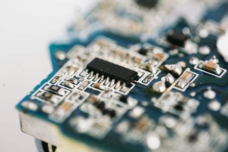
In the world of high-speed PCB design, differential pair impedance is a critical parameter that directly impacts signal integrity, data transmission reliability, and electromagnetic compatibility (EMC). Differential signaling, commonly used in protocols like USB 2.0/3.0, HDMI, PCIe, Ethernet, and LVDS, relies on two complementary traces carrying equal but opposite signals. The key challenge is to maintain a consistent differential impedance—typically 100Ω for most applications (e.g., USB, Ethernet) or 90Ω for specific standards (e.g., HDMI, DDR memory interfaces). Achieving these values requires precise control of trace geometry, stack-up design, and material selection.
This pillar content will guide you through the fundamentals of differential pair impedance, the step-by-step process to achieve 100Ω and 90Ω, and best practices for impedance control PCB fabrication. Whether you are a seasoned engineer or a newcomer to high-speed design, this comprehensive resource will help you avoid common pitfalls and ensure your prototype meets performance specifications.
Understanding Differential Pair Impedance
What Is Differential Impedance?
Differential impedance (Z_diff) is the impedance between the two traces of a differential pair when driven by a differential signal. It is mathematically defined as twice the odd-mode impedance (Z_odd), which is the impedance of each trace relative to the reference plane when both traces are driven with opposite polarities. In contrast, common-mode impedance (Z_cm) is the impedance of the pair when both traces carry identical signals. For most high-speed designs, the target is to match Z_diff to 100Ω or 90Ω to minimize reflections and signal degradation.
Key Factors Affecting Differential Impedance
Several variables influence differential pair impedance, and understanding them is essential for achieving precise control:
- Trace Width (W): Wider traces lower impedance; narrower traces increase impedance.
- Trace Spacing (S): Tighter spacing increases capacitive coupling, reducing differential impedance; wider spacing reduces coupling, increasing impedance.
- Dielectric Height (H): The distance between the trace layer and the reference plane (prepreg or core thickness) significantly impacts impedance. Thicker dielectrics increase impedance; thinner dielectrics decrease it.
- Dielectric Constant (Dk or Er): Higher Dk materials (e.g., FR4 with Dk ~4.5) reduce impedance; lower Dk materials (e.g., Rogers with Dk ~3.5) increase impedance.
- Copper Thickness (T): Thicker copper reduces impedance due to increased capacitance, but its effect is often secondary to width and spacing.
- Solder Mask and Surface Finish: Solder mask can lower impedance by 2–5Ω due to its higher Dk (~3.5–4.0), especially on fine-pitch designs. Surface finishes like ENIG or HASL also add minor effects.
Standard Target Values: 100Ω vs. 90Ω
100Ω Differential Impedance: The most common standard, used in USB (2.0, 3.0), Ethernet (100Base-T, Gigabit), LVDS, and many other high-speed interfaces. It offers a good balance between signal integrity and power consumption.
90Ω Differential Impedance: Required for HDMI, DisplayPort, and some DDR memory interfaces (e.g., DDR4/DDR5 differential clock pairs). The lower impedance reduces voltage swing and improves noise margin in these applications.
Why the difference? The choice between 100Ω and 90Ω is driven by protocol specifications, which are optimized for specific voltage levels, termination schemes, and cable impedances. For example, HDMI cables are standardized at 90Ω, while Ethernet cables are 100Ω. Using the wrong impedance can cause reflections, signal loss, and compliance failures.
Step-by-Step Guide to Achieving 100Ω and 90Ω in Impedance Control PCB
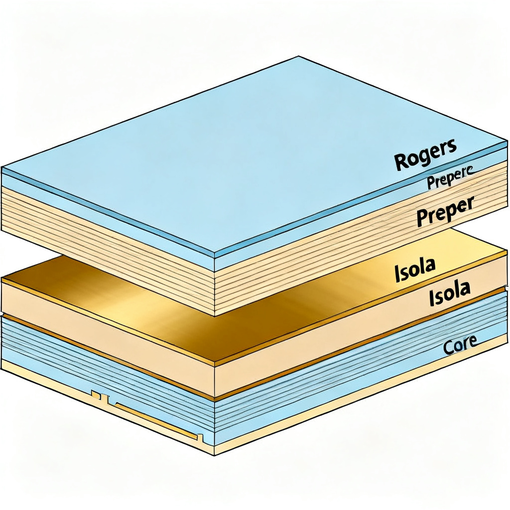
Pre-Design Planning: Stack-Up and Material Selection
The first step is to define your PCB stack-up, which determines the dielectric height and layer arrangement. For differential pairs, you typically route them on the same layer with a continuous reference plane (ground or power) directly below. Common stack-up options include:
- 4-Layer Stack-Up: Signal-Ground-Power-Signal (for low-cost designs). Use the top layer for differential pairs with a ground plane on layer 2.
- 6-Layer or More: For high-speed designs, place differential pairs on outer layers with adjacent ground planes to minimize crosstalk and EMI.
Material Selection: FR4 is cost-effective but has a wide Dk tolerance (4.2–4.8). For precise impedance control PCB, use low-loss materials like Rogers 4350B (Dk ~3.48), Isola 370HR (Dk ~4.0), or high-speed FR4 variants (e.g., ITEQ IT-180A). Always request a controlled impedance test coupon from your manufacturer to verify.
Calculating Trace Geometry
Use impedance calculation tools (e.g., Polar SI9000, Saturn PCB Toolkit, or Altium Designer’s impedance calculator) to determine the required trace width (W) and spacing (S) for your target impedance. The formula for differential impedance (microstrip or stripline) is:
For Edge-Coupled Microstrip (outer layer):
Z_diff ≈ 2 * Z_0 * (1 – 0.48 * e^(-0.96 * (S/H)))
For Broadside-Coupled Stripline (inner layer):
Z_diff = 2 * Z_0 * (1 – 0.374 * e^(-2.9 * (S/H)))
Where Z_0 is the characteristic impedance of a single trace (typically 50Ω for single-ended), and H is the dielectric height.
Example for 100Ω Microstrip (FR4, Dk=4.5, H=4 mil, T=1 oz copper):
- Single-ended impedance: ~55Ω (from calculator)
- To achieve Z_diff = 100Ω, set W = 6 mil, S = 8 mil (typical values; adjust based on tool).
- Reduce spacing (S) to 6 mil to lower impedance to 90Ω, or increase width (W) to 7 mil.
Example for 90Ω Stripline (inner layer, H=8 mil, Dk=4.0):
- Single-ended impedance: ~50Ω
- For Z_diff = 90Ω, use W = 5 mil, S = 10 mil. Tighten spacing to 7 mil for 100Ω.
Key Insight: Always simulate with your specific stack-up and material Dk. Manufacturers often provide recommended geometries for their processes.
Accounting for Manufacturing Tolerances
PCB fabrication introduces variations in etching (trace width tolerance ±10–20%), dielectric thickness (±10%), and copper thickness (±0.5 oz). To ensure your design meets impedance targets:
- Design for 5–10% margin: Aim for Z_diff = 95–105Ω for 100Ω target, and 85–95Ω for 90Ω target.
- Use impedance coupons: Include test coupons on the panel edge for measurement by the manufacturer. Request a report showing actual measured impedance.
- Select a reputable manufacturer: Choose a PCB fabricator with experience in controlled impedance, such as Sierra Circuits, PCBWay, or JLCPCB (for simpler designs). They offer impedance control services with tolerances of ±10% or better.
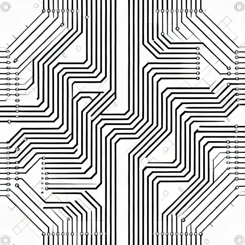
Practical Tips for Routing Differential Pairs
Keep pairs symmetrical: Both traces should have identical length, width, and spacing. Avoid bends that create asymmetry; use 45-degree or arc bends instead of 90-degree corners.
Minimize vias: Each via adds inductance and capacitance, altering impedance. If vias are unavoidable, use ground stitching vias nearby to maintain return path continuity.
Maintain constant spacing: Avoid varying S along the trace. Use “neck-down” regions only when necessary (e.g., near BGA pads) and compensate with length tuning.
Reference plane continuity: Ensure a solid ground plane beneath the pair. Avoid splits or gaps; if crossing a split, use stitching capacitors.
Length matching: For differential pairs, match trace lengths to within 5–10 mils to minimize skew. Use serpentine patterns for tuning.
Advanced Considerations for High-Speed PCB
Impedance vs. Frequency: Why It Matters
At high frequencies (above 1 GHz), differential pair impedance can vary due to skin effect, dielectric loss, and frequency-dependent Dk. For example, FR4’s Dk drops from ~4.5 at 1 MHz to ~4.2 at 10 GHz, causing impedance to increase by 2–5Ω. To maintain 100Ω or 90Ω across the frequency range:
- Use low-loss materials with stable Dk (e.g., Rogers, Megtron 6).
- Simulate with frequency-dependent models in tools like Ansys HFSS or Keysight ADS.
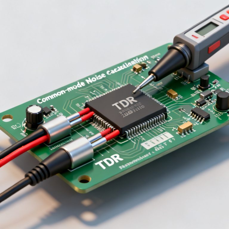
- Request wideband impedance testing (TDR) from your manufacturer.
Impact of Solder Mask and Surface Finish
Solder mask reduces differential impedance by 2–5Ω, depending on its thickness and Dk (typically 3.5–4.0). For fine-pitch designs (e.g., 0.5 mm BGA), the effect is more pronounced. To compensate:
- Increase trace spacing (S) by 1–2 mils or reduce trace width (W) by 0.5–1 mil.
- Use “solder mask defined” pads only when necessary; prefer non-solder mask defined (NSMD) pads for impedance control.
- Surface finishes like ENIG (electroless nickel immersion gold) add negligible impedance change, but HASL (hot air solder leveling) can alter trace geometry.
Common Pitfalls and How to Avoid Them
Ignoring return path: A differential pair without a continuous ground plane below will have uncontrolled impedance. Always ensure a reference plane (ground or power) within 2–3 dielectric layers.
Incorrect termination: Even with perfect impedance, improper termination (e.g., missing or wrong resistor values) causes reflections. Use 100Ω termination resistors for 100Ω lines, or 90Ω for 90Ω lines.
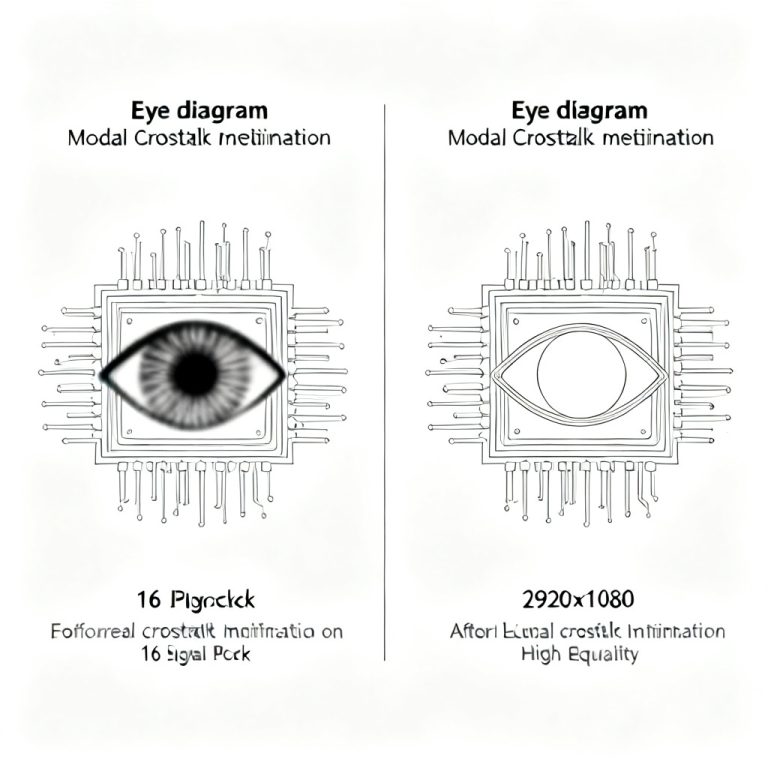
Overlooking coupling to adjacent traces: Keep at least 3x the trace width (3W) spacing between differential pairs to minimize crosstalk.
Assuming FR4 is sufficient for high-speed: For designs above 5 Gbps, FR4’s high loss and Dk variation can degrade performance. Upgrade to low-loss materials.
Manufacturer Collaboration and Verification
Communicating with Your PCB Fabricator
To achieve reliable impedance control PCB, provide your manufacturer with:
- Stack-up diagram: Specify layer order, material type, and dielectric thickness.
- Impedance targets: Clearly state 100Ω or 90Ω for each differential pair.
- Trace geometry: Include target W and S, but allow the manufacturer to adjust based on their process.
- Test coupon requirements: Request impedance coupons per IPC-2141A standard.
Testing and Validation
After fabrication, verify impedance using:
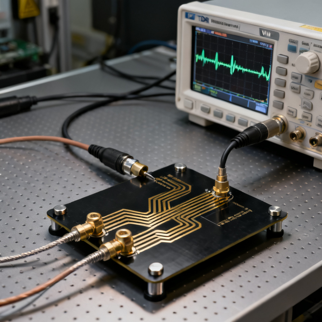
- Time Domain Reflectometry (TDR): The most accurate method, measuring impedance along the trace length. A typical TDR plot shows impedance variations due to bends, vias, or manufacturing defects.
- Vector Network Analyzer (VNA): For S-parameter measurements (e.g., S11, S21) up to 20 GHz.
- Impedance coupon testing: The manufacturer provides a report with measured values; compare to your target.
Acceptance Criteria: For 100Ω, a range of 95–105Ω is typical; for 90Ω, 85–95Ω. Tighter tolerances (±5%) are possible with premium materials and processes.
Case Studies and Real-World Examples
Case Study: 100Ω for USB 3.0
A client required a 4-layer board for USB 3.0 (5 Gbps) with 100Ω differential pair impedance. Using FR4 (Dk=4.5), we designed a microstrip pair on top layer with W=6 mil, S=8 mil, H=4 mil (prepreg). The manufacturer reported TDR results of 98–102Ω across all pairs. Key success factors: consistent spacing, ground plane on layer 2, and avoidance of vias near the connector.
Case Study: 90Ω for HDMI 2.1
For an HDMI 2.1 design (48 Gbps), we used a 6-layer stack-up with Rogers 4350B (Dk=3.48) for inner-layer stripline pairs. Target W=5 mil, S=10 mil, H=8 mil. After fabrication, impedance measured 88–92Ω, within spec. The low-loss material minimized signal attenuation at 12 GHz.
Industry Terminology Glossary
Differential Pair Impedance (Z_diff): The impedance between two traces carrying equal but opposite signals, critical for high-speed data integrity.
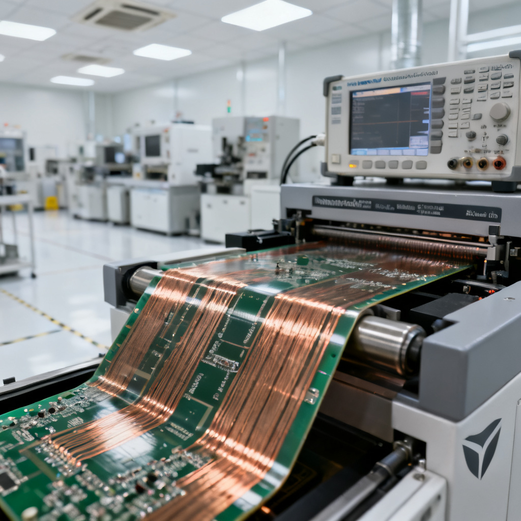
Impedance Control PCB: A printed circuit board manufactured with tight tolerances on trace geometry and dielectric properties to achieve target impedance values.
Odd-Mode Impedance (Z_odd): The impedance of one trace in a differential pair when driven opposite to the other, typically half of Z_diff.
Dielectric Constant (Dk): A material property that affects signal propagation speed and impedance; lower Dk yields higher impedance.
Time Domain Reflectometry (TDR): A testing method that measures impedance along a trace by sending a fast pulse and analyzing reflections.
Comparison: Our High-Speed PCB Services vs. Standard Fabricators
| Feature | Standard PCB Fabricator | Our High-Speed Impedance Control PCB Service |
|---|---|---|
| Differential Pair Impedance Tolerance | ±15% to ±20% | ±5% to ±10% |
| Material Options for 100Ω/90Ω | FR4 only | FR4, Rogers, Isola, Megtron |
| Impedance Testing | Coupon only (optional) | Coupon + TDR (included) |
| Stack-Up Design Support | Basic | Advanced simulation-based |
| Lead Time for Controlled Impedance | Standard | Expedited with priority |
Conclusion: Mastering Differential Pair Impedance
Achieving 100Ω or 90Ω differential pair impedance is a blend of careful design, material selection, and manufacturer collaboration. By understanding the influencing factors—trace geometry, stack-up, and material Dk—you can ensure your impedance control PCB performs reliably. Remember to simulate, test, and iterate. For complex designs, partner with an experienced PCB manufacturer who offers controlled impedance services.
At [Your Company Name], we specialize in high-speed PCB fabrication with precise impedance control. Our advanced stack-up capabilities, low-loss materials, and rigorous testing ensure your prototypes meet 100Ω and 90Ω targets. Contact us today for a free design review and quote.
Frequently Asked Questions (FAQ)
What is the difference between 100Ω and 90Ω differential pair impedance?
Differential pair impedance of 100Ω is standard for USB, Ethernet, and LVDS, while 90Ω is used for HDMI, DisplayPort, and DDR memory. The choice depends on the protocol’s voltage and termination requirements. Using the wrong impedance can cause signal reflections in your impedance control PCB.
How do I calculate trace width for 100Ω differential impedance?
Use an impedance calculator (e.g., Polar SI9000) with your stack-up parameters (dielectric height, Dk, copper thickness). For a typical FR4 microstrip with H=4 mil, target W=6 mil and S=8 mil for 100Ω differential pair impedance. Adjust based on manufacturer recommendations.
Can FR4 achieve 90Ω differential impedance reliably?
Yes, FR4 can achieve 90Ω differential pair impedance with careful design, but its Dk variation (±0.3) may cause tolerance issues. For precise 90Ω, consider low-loss materials like Rogers or Isola, especially for high-speed impedance control PCB designs above 5 Gbps.
Why does solder mask affect differential impedance?
Solder mask has a higher dielectric constant (Dk ~3.5–4.0) than air, which increases capacitance and lowers differential pair impedance by 2–5Ω. Compensate by adjusting trace spacing or width in your impedance control PCB layout.
What is the best way to verify impedance on a prototype?
Use Time Domain Reflectometry (TDR) testing on impedance coupons or actual traces. Request a TDR report from your impedance control PCB manufacturer to ensure values are within 95–105Ω for 100Ω targets or 85–95Ω for 90Ω targets.
“`