Master impedance control for high-speed PCBs. This definitive guide covers the complete workflow for impedance control PCB simulation in Ansys Q2D Extractor, from geometry import and material stackup definition to differential pair simulation and result interpretation for manufacturing.
Why Impedance Control Simulation Matters for High-Speed PCBs
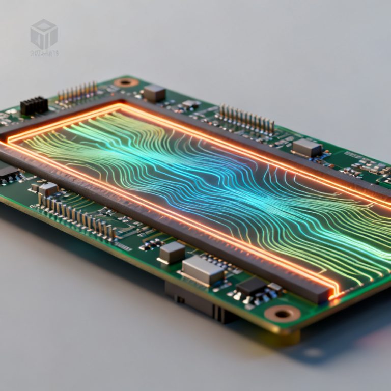
In the world of high-speed digital design, signal integrity is paramount. Controlled impedance is no longer a luxury; it is a fundamental requirement for preventing signal reflection, crosstalk, and electromagnetic interference (EMI) in modern PCBs operating at GHz frequencies. Without precise impedance matching, your high-speed design—whether for DDR memory, PCIe, or RF circuits—will fail to perform. Impedance control PCB simulation in Ansys Q2D Extractor is the industry-standard 2D field solver for calculating the characteristic impedance, resistance, capacitance, and inductance of transmission line cross-sections.
Step 1: Project Setup and Geometry Import for Impedance Control PCB Simulation
The foundation of any accurate impedance control PCB simulation in Ansys Q2D Extractor is a correct model of the PCB cross-section. You have two primary paths to create this geometry in Q2D Extractor.
Method A: Manual Geometry Creation (Best for Pre-Layout Stackup Planning)
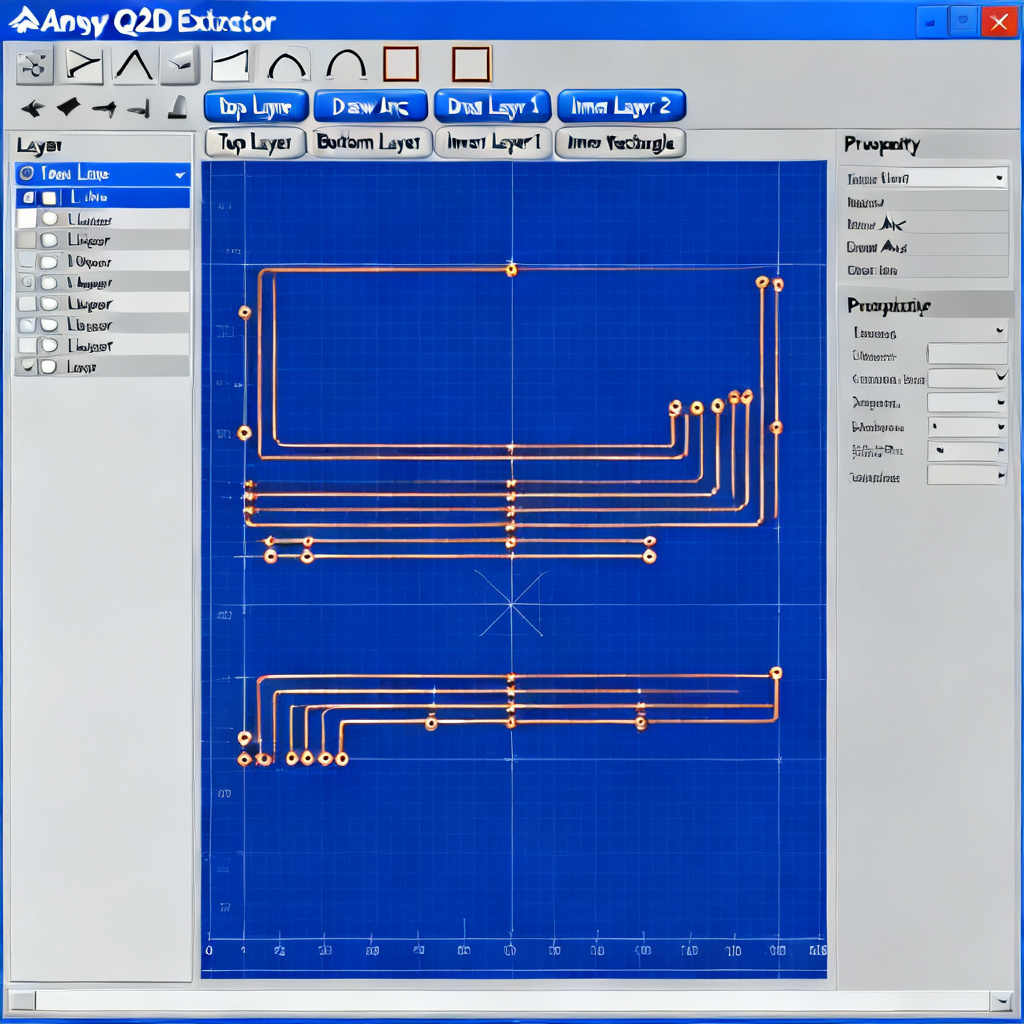
This method is ideal when you are designing a new stackup and have not yet routed the board. Launch Q2D Extractor from the Ansys Electronics Desktop suite. Create a new project via Project > Insert Q2D Extractor Design. Define the solution type as AC for most high-speed digital applications. Draw rectangles for each dielectric layer (e.g., Core, Prepreg) using the Draw menu, ensuring you draw them from top to bottom in the correct physical order. Assign material properties like dielectric constant (Dk) and loss tangent (Df) to each layer. Draw the copper traces using the Draw > Line or Rectangle tool, paying close attention to accurate trace thickness (e.g., 1 oz copper = 0.035mm).
Method B: Importing Layout from Altium, Cadence, or Allegro
This method is for post-layout verification. Export the cross-section of your selected trace from your EDA tool as an Ansys Neutral File (.anf) or ODB++ file. Import this file into Q2D via File > Import. Carefully verify the imported geometry, ensuring all layers are aligned and trace dimensions match your PCB layout.
Step 2: Defining Material Properties and Layer Stackup for Impedance Control
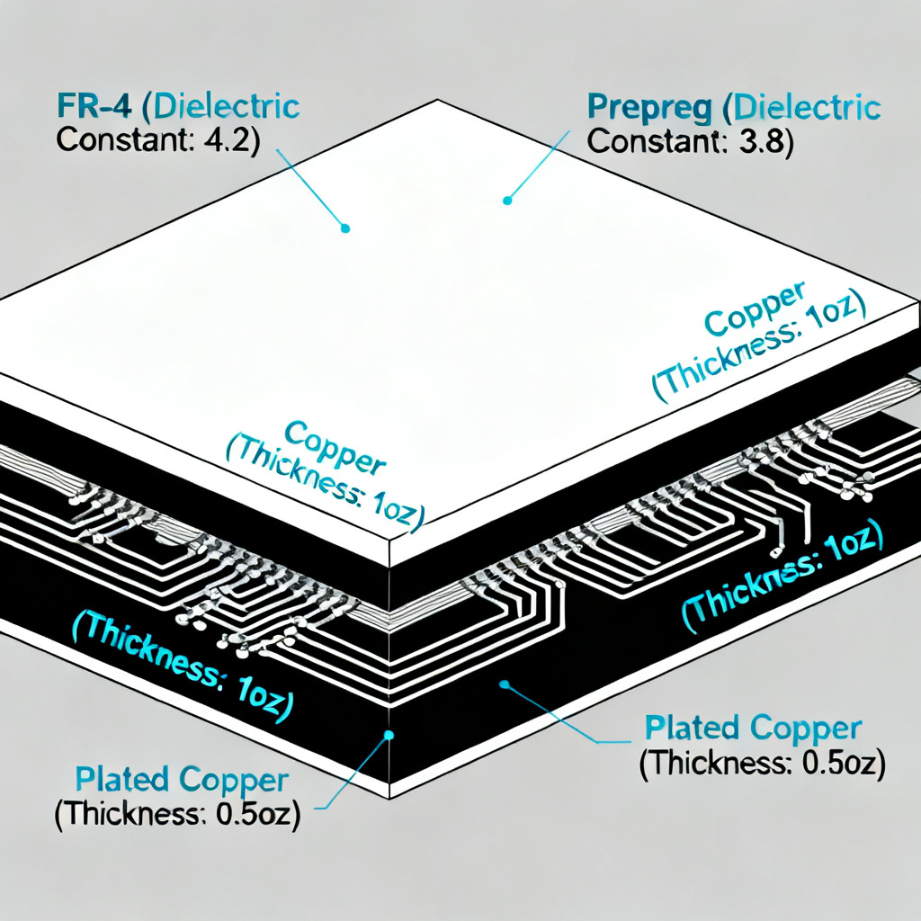
This is the single most critical step for accuracy. The dielectric constant (Dk) of your laminate material directly determines the impedance. Access the material library via Tools > Edit Configured Libraries. Assign materials to each dielectric rectangle, setting both permittivity (Dk) and loss tangent (Df) at your operating frequency. For standard FR4, Dk is typically between 4.2 and 4.5 at 1 GHz, while Df is around 0.02. For high-speed materials like Megtron 6, Df can be as low as 0.002. The distance (H) between the signal trace and its reference plane is the dominant factor controlling impedance. Include copper roughness effects using models like Huray or Hammerstad for advanced accuracy.
Step 3: Setting Up Excitations and Boundaries for Impedance Control PCB Simulation
This step tells Q2D what you are measuring and the electrical environment. Select your signal trace rectangle and assign Signal Line excitation. Select the reference planes (ground layers) and assign Ground excitation. For differential pairs (e.g., USB, HDMI, LVDS), draw two traces with correct width (W) and spacing (S). Assign Signal Line to both, then create a differential pair from the two terminals in the Excitations menu. Q2D will calculate odd-mode impedance (Zdiff) and common-mode impedance (Zcom). For a microstrip, ensure the background is set to Vacuum or Air. Use a Symmetry boundary for perfectly symmetrical differential pairs to reduce solve time.
Step 4: Running the Simulation and Analyzing Results
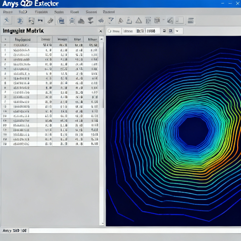
Once the model is set up, create a solution setup with an appropriate frequency sweep (e.g., single point for 1 GHz, interpolating for DC-20 GHz). Increase mesh refinement for high accuracy. Validate the setup and run the simulation. The key results include Z0 (characteristic impedance for single-ended traces, target ~50 ohms) and Zdiff (differential impedance, target ~100 ohms). Review field plots (E-field and H-field) to diagnose crosstalk or field confinement issues.
Step 5: Linking Impedance Control PCB Simulation to Manufacturing
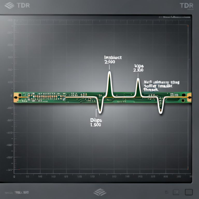
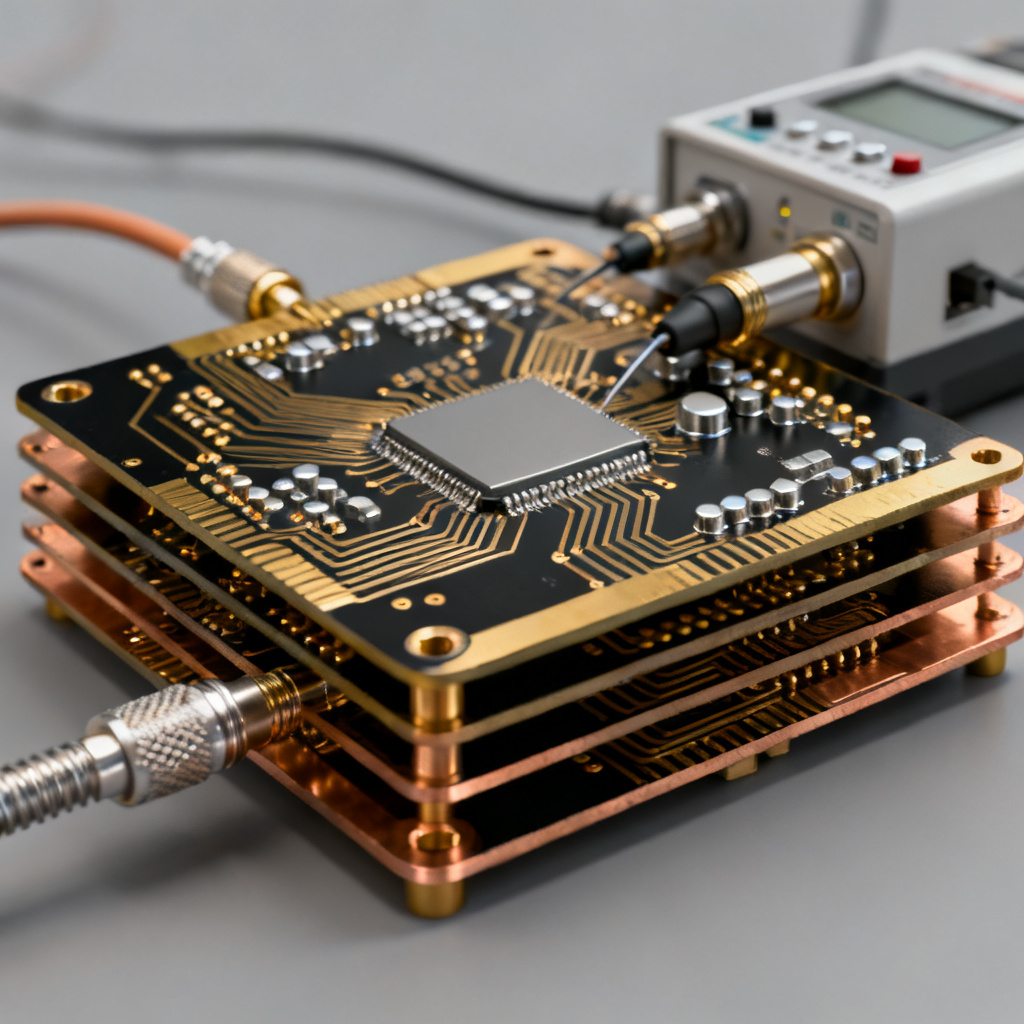
The most accurate impedance control PCB simulation in Ansys Q2D Extractor is useless if your manufacturer cannot replicate it. Provide a target impedance with a tolerance (e.g., 50 ohms ± 5%). Perform a “what-if” analysis by parameterizing trace width (W) and dielectric height (H) to model manufacturing variations. Create a stackup table for your fabricator, listing trace type, target impedance, width, spacing, material, and height. Finally, correlate your simulation with Time Domain Reflectometry (TDR) measurements from production coupons.
Frequently Asked Questions (FAQ) About Impedance Control PCB Simulation in Ansys Q2D Extractor
What is the primary purpose of impedance control PCB simulation in Ansys Q2D Extractor?
The primary purpose is to accurately calculate the characteristic impedance of transmission lines on a PCB, ensuring signal integrity for high-speed designs.
How do I set up a differential pair for impedance control PCB simulation in Ansys Q2D Extractor?
Draw two traces with the correct width and spacing, assign both as Signal Line excitations, and then create a differential pair from the two terminals in the Excitations menu.
What is the most critical factor affecting impedance in a PCB stackup?
The distance (H) between the signal trace and its nearest reference plane is the dominant factor. The dielectric constant (Dk) of the material is also highly critical.
How can I ensure my simulation matches the actual manufactured PCB?
Provide your manufacturer with a target impedance and tolerance, perform sensitivity sweeps on trace width and dielectric height, and request TDR measurements on production coupons for correlation.
Impedance Control PCB Simulation: Parameter Comparison Table
| Parameter | Typical Value for 50 Ohm Microstrip | Impact on Impedance Control PCB Simulation |
|---|---|---|
| Trace Width (W) | 8.5 mils | Wider trace = lower impedance; narrower = higher impedance. |
| Dielectric Height (H) | 4.0 mils | Larger H = higher impedance; smaller H = lower impedance. |
| Dielectric Constant (Dk) | 4.3 (FR4 at 1 GHz) | Higher Dk = lower impedance; lower Dk = higher impedance. |
| Copper Thickness (T) | 1.4 mils (1 oz) | Thicker copper = slightly lower impedance. |
| Target Impedance | 50 ohms ± 5% | Must be achieved for signal integrity. |
Key Terminology for Impedance Control PCB Simulation
- Characteristic Impedance (Z0): The impedance a signal sees when traveling along a uniform transmission line.
- Differential Impedance (Zdiff): The impedance seen by a signal on a pair of coupled traces.
- Odd-mode Impedance: The impedance of one line in a differential pair when driven in opposite polarity.
- Dielectric Constant (Dk): A measure of a material’s ability to store electrical energy, directly affecting signal propagation speed and impedance.
- Loss Tangent (Df): A measure of signal loss in the dielectric material.
- Time Domain Reflectometry (TDR): A measurement technique used to verify the impedance of a manufactured PCB.
“`