In high-speed PCB design, identifying aggressor vs victim nets is essential for managing crosstalk and ensuring signal integrity. This pillar content provides a comprehensive framework to pinpoint critical crosstalk pairs, drawing from expert sources like Altium, Sierra Circuits, and Cadence, to help you design reliable boards for your B2B clients.
1. Fundamentals of Aggressor and Victim Nets in High Speed PCB
1.1 Definition and Roles of Aggressor vs Victim Nets
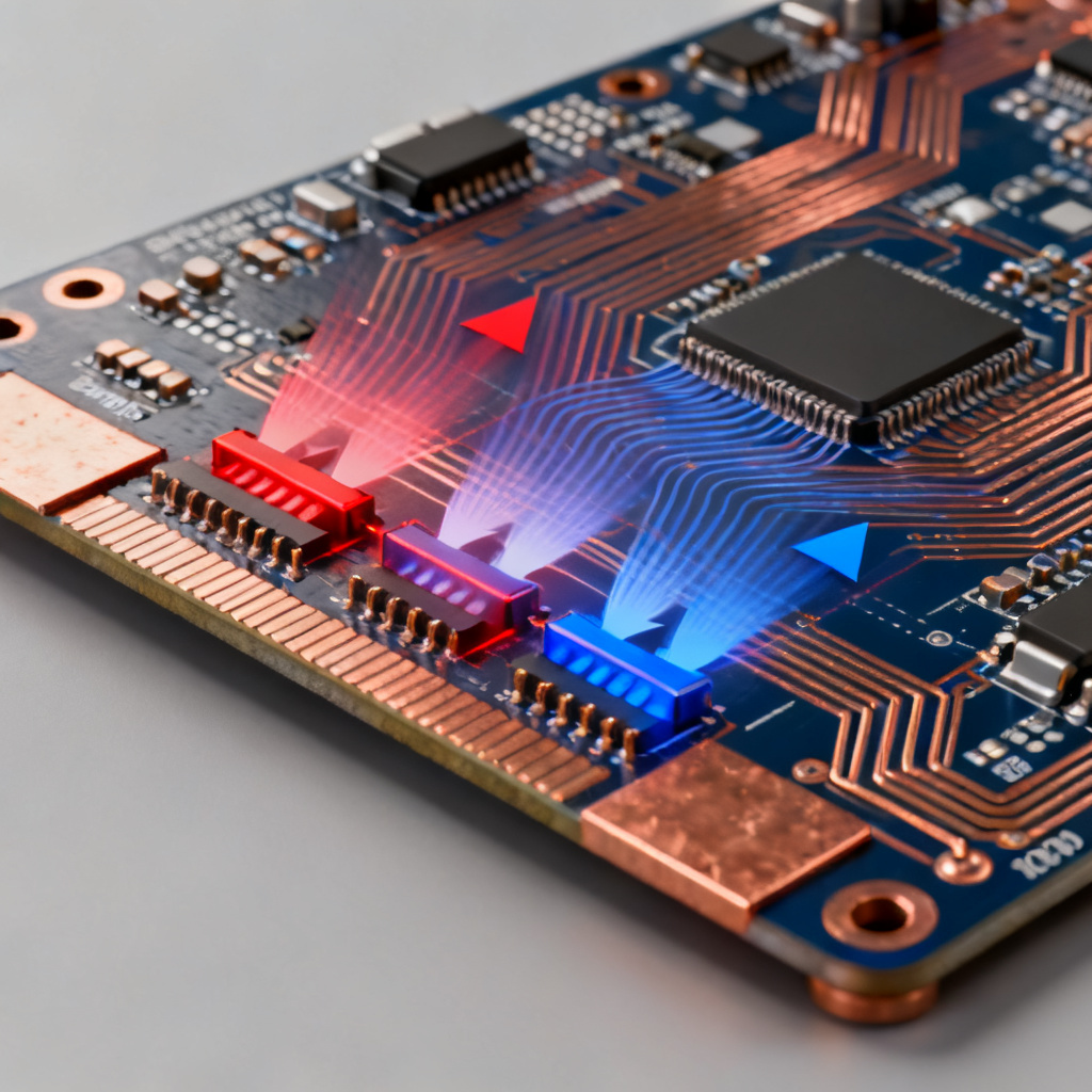
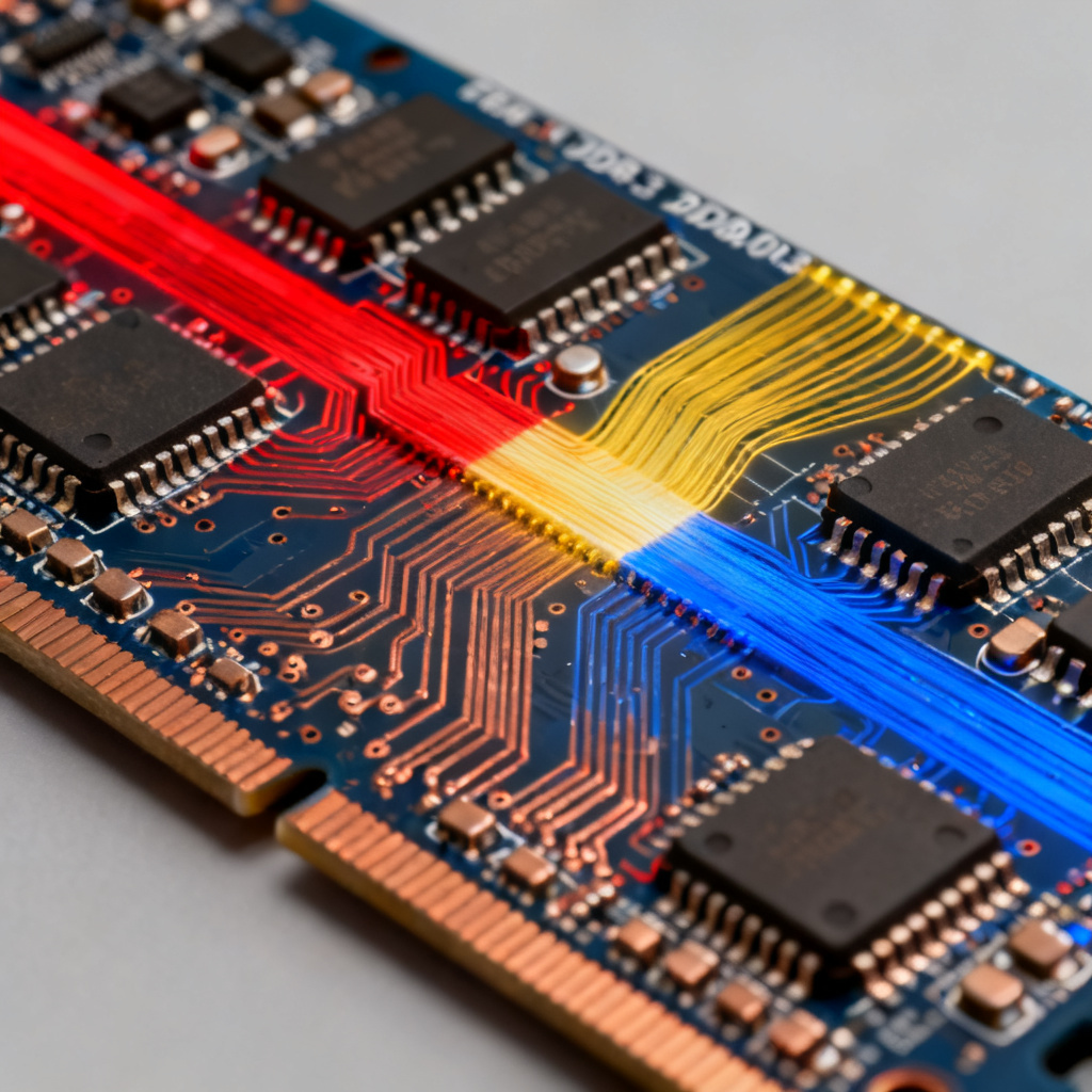
Aggressor vs victim nets define the source and receiver of crosstalk in high speed PCB design. An aggressor net is typically a fast-switching signal like a clock or data bus, while a victim net is a sensitive trace such as an analog input or low-speed control line. The coupling occurs via capacitive or inductive fields, with inductive coupling dominating at high frequencies due to mutual inductance between parallel traces.
1.2 Key Characteristics of Critical Pairs in High Speed PCB
Critical aggressor vs victim nets share three traits: proximity (spacing less than 3x dielectric height), parallel length (over 1 inch), and fast signal edge rates (below 500 ps). For example, a 1V/ns edge rate can induce up to 100 mV of noise on a victim net within 1 cm of parallel routing. These characteristics make them a top priority in high speed PCB design.
1.3 The Role of Impedance and Termination in High Speed PCB Crosstalk
Impedance mismatch at the victim net’s receiver can worsen crosstalk in high speed PCB systems. If the victim net is unterminated or has high input impedance (e.g., >10 kΩ), reflected energy from the aggressor’s coupling can create standing waves. Proper termination, such as a 50-ohm resistor, can reduce crosstalk amplitude by up to 40% compared to an open circuit, making it a key factor in managing aggressor vs victim nets.
2. Identifying Critical Crosstalk Pairs in High Speed PCB: A Step-by-Step Approach
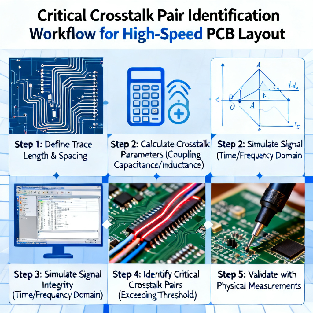
2.1 Step 1: Map Your Net Hierarchy for High Speed PCB
To identify critical aggressor vs victim nets, create a net classification based on signal type and sensitivity. High-risk aggressors include clocks (e.g., 100 MHz+), DDR data lines, and high-speed serial links. High-risk victims include analog signals (e.g., ADC inputs), reset lines, and low-frequency I2C or SPI buses. Use a spreadsheet or PCB design tool to tag each net with its role in the high speed PCB.
2.2 Step 2: Evaluate Physical Proximity and Geometry in High Speed PCB
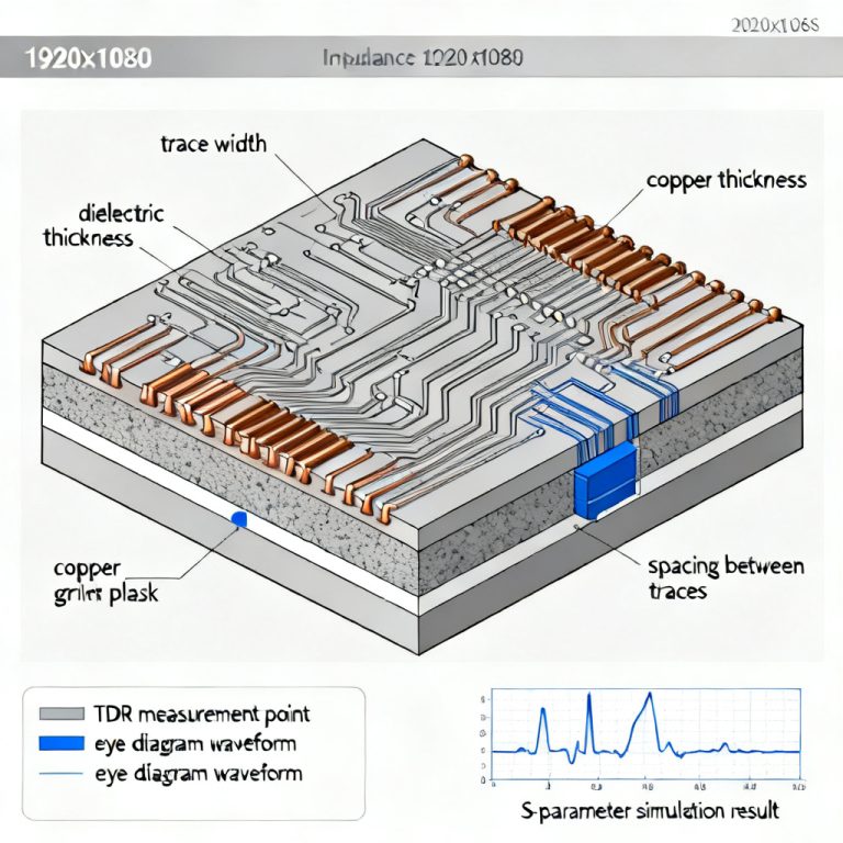
Apply the “3W Rule” as a baseline for spacing in high speed PCB, but for critical pairs, consider the S/H ratio. For microstrip, critical coupling occurs when S/H < 2, where H is the distance to the reference plane. For stripline, crosstalk is 50-70% lower, but parallel lengths over 2 inches still pose risks. Via proximity also matters: vias from aggressor nets can couple to victim vias if spaced <5 mils edge-to-edge in a high speed PCB stack.
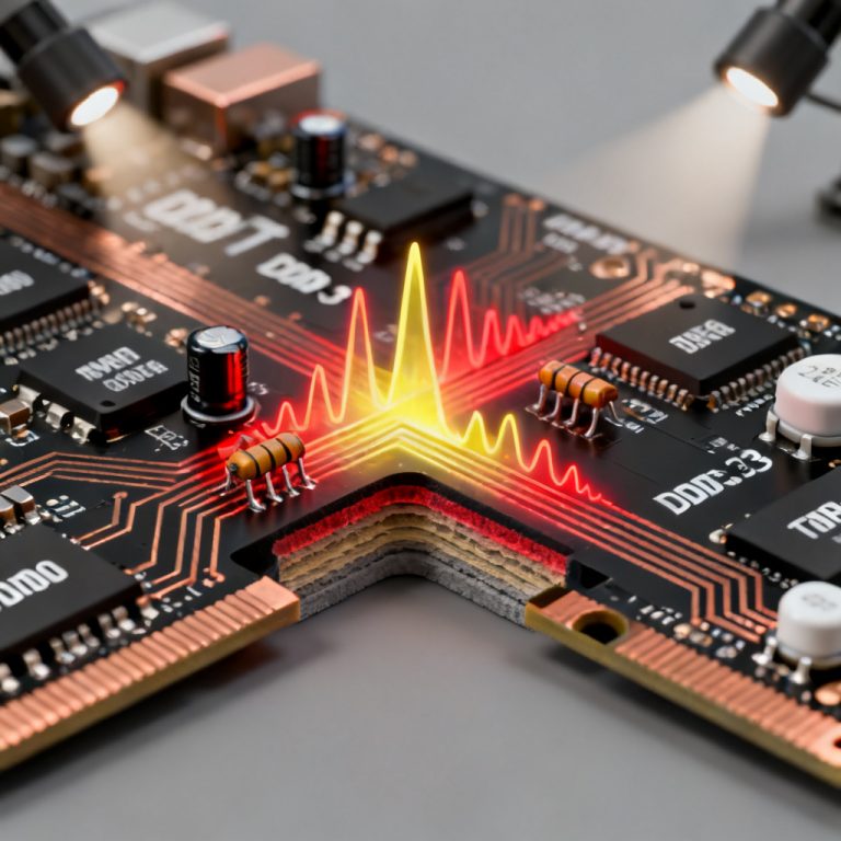
2.3 Step 3: Analyze Timing and Noise Margins in High Speed PCB
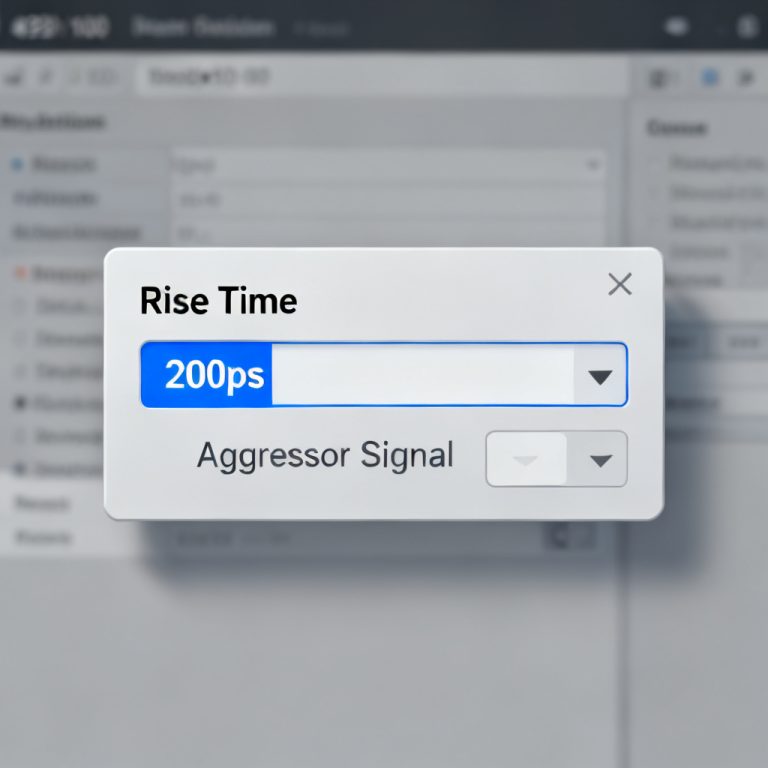
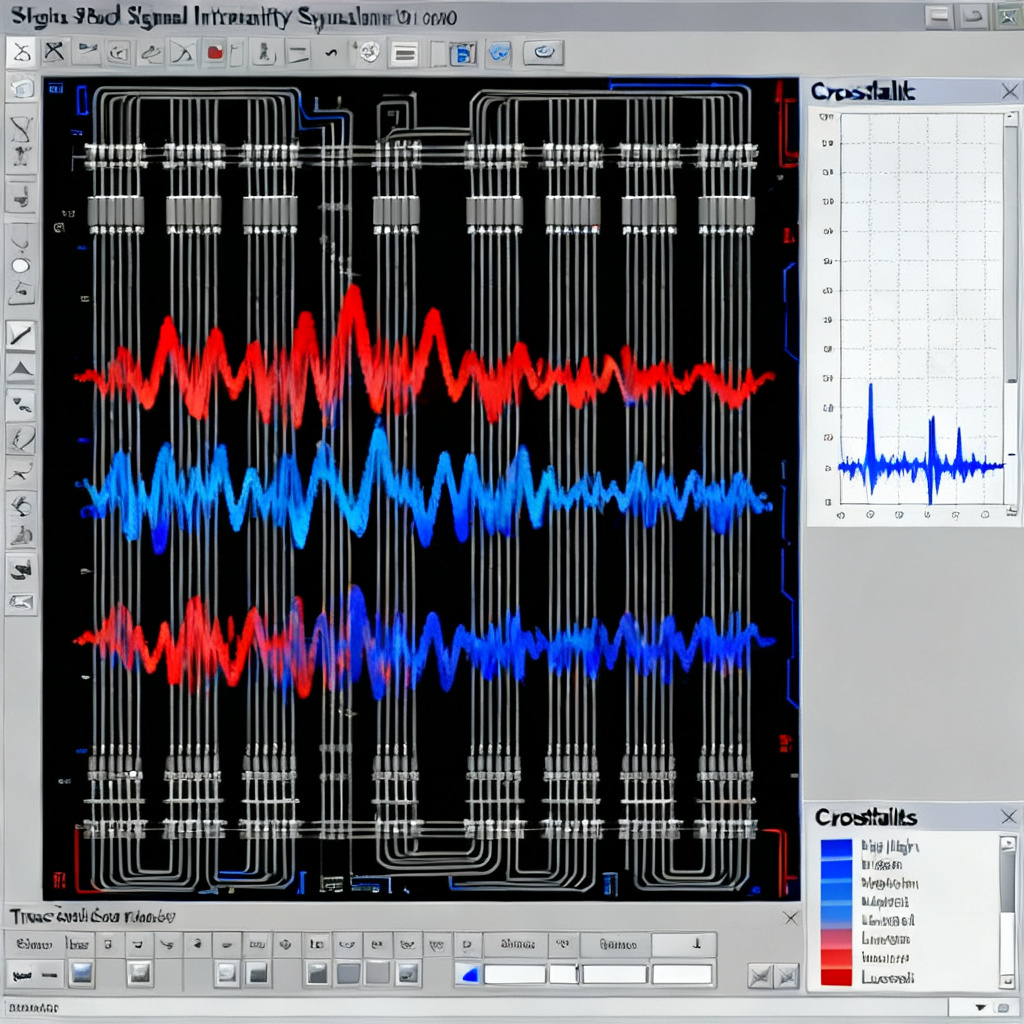
Use signal integrity simulations to quantify crosstalk in high speed PCB designs. Near-End Crosstalk (NEXT) appears at the aggressor’s source end, while Far-End Crosstalk (FEXT) appears at the victim’s far end. For a 500 ps rise time, NEXT can exceed 5% of the aggressor’s voltage swing if S/H < 1.5. Check noise margins: a victim net with a 200 mV noise margin can tolerate up to 50 mV of crosstalk, but a 1.8V CMOS input with 100 mV margin may fail at 30 mV. Prioritize pairs where crosstalk exceeds 10% of the victim’s noise margin in high speed PCB analysis.
2.4 Step 4: Use Coupling Coefficient Thresholds for High Speed PCB
Define a coupling coefficient (K) threshold for aggressor vs victim nets in high speed PCB. For microstrip, K > 0.1 indicates critical coupling. A practical rule: if the aggressor’s edge rate (tr) is less than 2x the time of flight (Tf) across the parallel segment (tr < 2*Tf), the pair is critical. Example: A 1-inch parallel run on FR4 (Tf~180 ps) with tr=300 ps gives tr/Tf=1.67, below the threshold—high risk for high speed PCB designs.
3. Real-World Examples of Critical Crosstalk Pairs in High Speed PCB
3.1 Example 1: DDR3 Memory Bus in High Speed PCB
In a high speed PCB, an aggressor (data strobe DQS at 800 MHz, 400 ps rise time) and victim (address line ADDR) running parallel for 1.5 inches on the same layer caused FEXT to reach 120 mV, exceeding the DDR3’s 90 mV noise margin. Solution: Increase spacing to 4x W and add a ground via fence between the aggressor vs victim nets.
3.2 Example 2: Mixed-Signal Design with ADC in High Speed PCB
In a high speed PCB, an aggressor (SPI clock SCLK at 50 MHz, 2 ns rise time) coupled 15 mV noise into a victim (16-bit ADC analog input), reducing effective resolution to 12 bits. Mitigation: Route SCLK on a different layer with a ground plane shield and use a series resistor (22 ohms) at the aggressor’s source to slow the edge rate to 5 ns, protecting the victim net in high speed PCB.
3.3 Example 3: High-Speed Serial Link in High Speed PCB
For a high speed PCB with PCIe Gen 3 (8 Gbps, 30 ps rise time), crosstalk between adjacent differential pairs created jitter >0.3 UI, violating the 0.15 UI spec. Solution: Increase inter-pair spacing to 5x the trace width and use differential routing with 100-ohm impedance control, reducing crosstalk between aggressor vs victim nets.
4. Mitigation Strategies for Critical Pairs in High Speed PCB
4.1 Spacing and Shielding for High Speed PCB Crosstalk
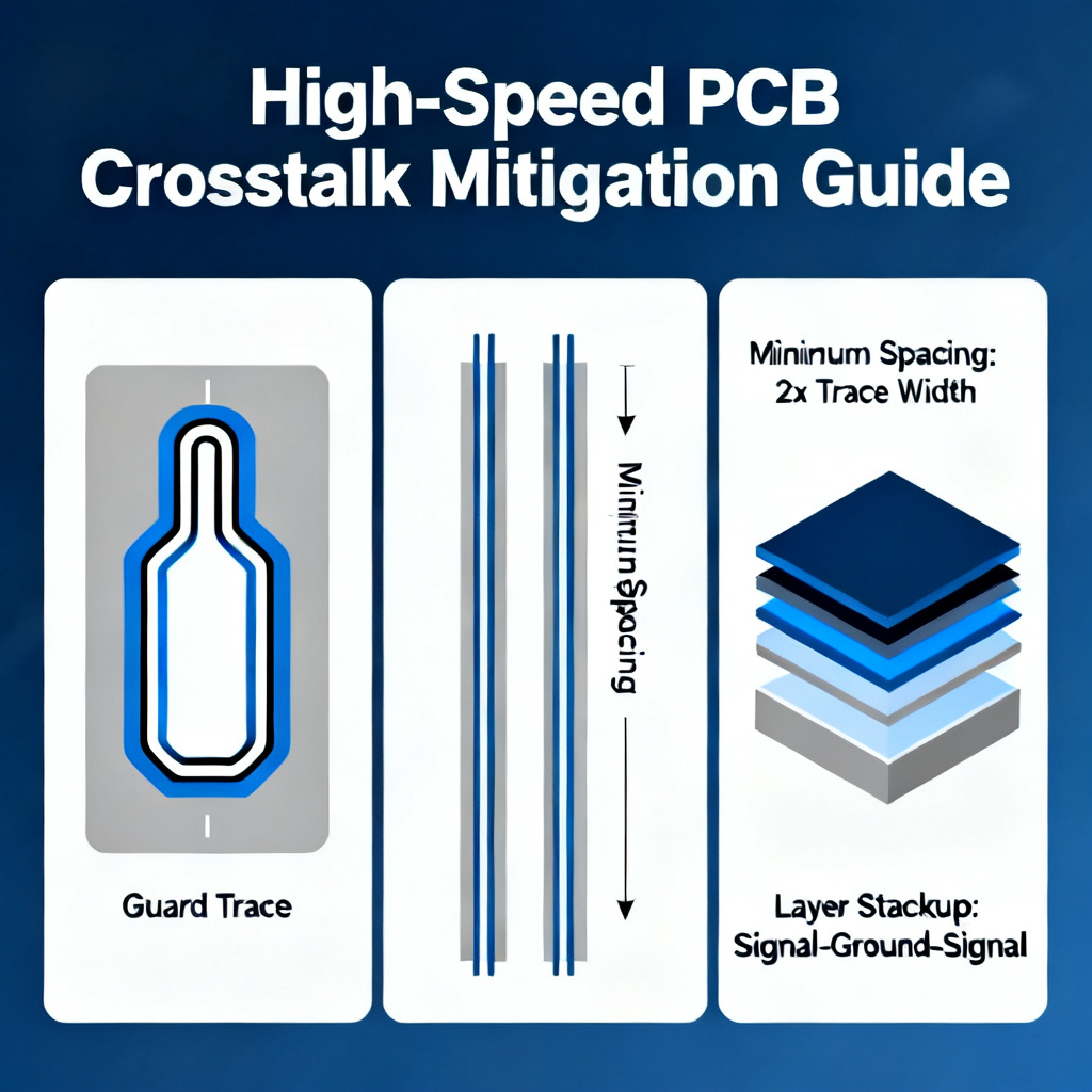
Place a grounded guard trace between aggressor vs victim nets in high speed PCB, spaced at least 2x W from each. This reduces capacitive coupling by 60-80% if the guard trace is stitched to ground via every 1/10 wavelength (e.g., every 150 mils for a 1 GHz signal). Layer separation also helps: route aggressors on inner layers (stripline) and victims on outer layers, with a ground plane between them, cutting crosstalk by 90%.
4.2 Edge Rate Control for High Speed PCB
Add series termination (10-50 ohms) at the aggressor’s driver to slow the rise time in high speed PCB. For example, a 33-ohm resistor on a 50-ohm line can increase tr from 200 ps to 500 ps, reducing crosstalk by 60%. Ferrite beads on victim nets (e.g., analog inputs) filter high-frequency noise without affecting signal bandwidth in high speed PCB designs.
4.3 Routing Topology for High Speed PCB
Avoid long parallel runs for aggressor vs victim nets in high speed PCB. Use a “staggered” or “serpentine” routing pattern for pairs that must cross. For differential pairs, maintain tight coupling within the pair (spacing = 1x W) to reduce external crosstalk, but increase inter-pair spacing to >3x W in high speed PCB layouts.
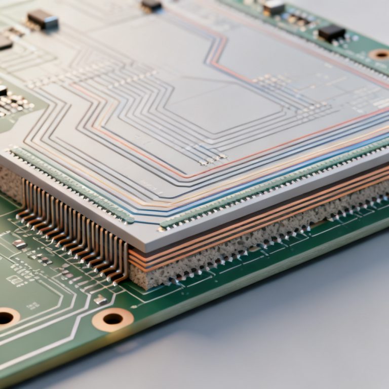
4.4 Stack-Up Optimization for High Speed PCB
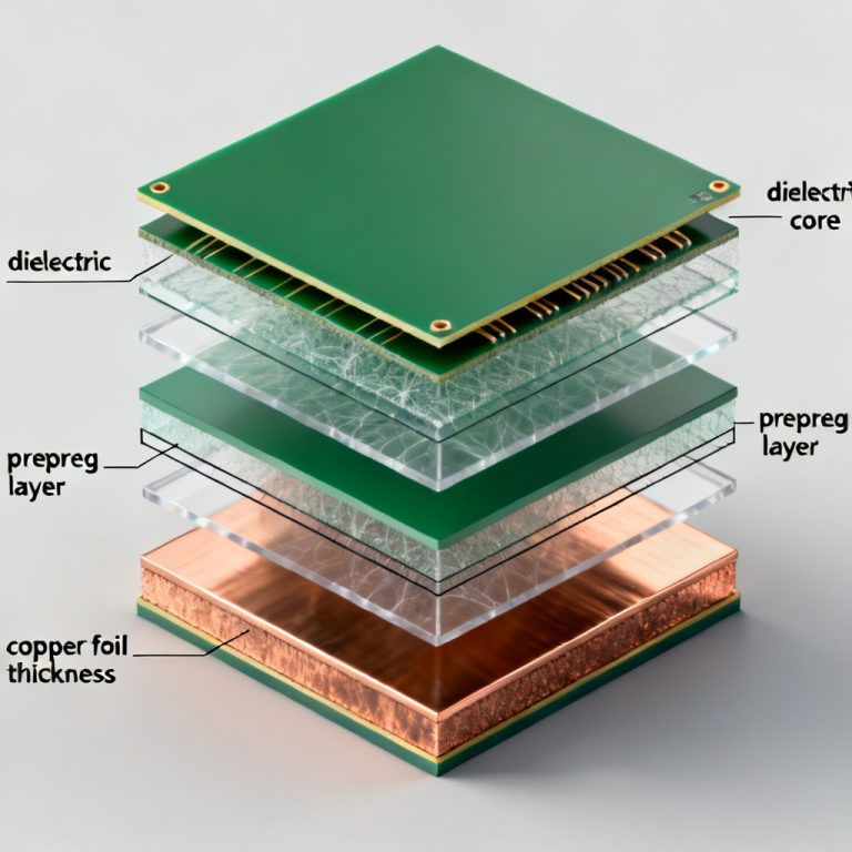
Use thin dielectrics to reduce H (distance to reference plane) in high speed PCB. For example, using 4-mil prepreg instead of 8-mil reduces microstrip crosstalk by 50%. In a 4-layer stack, place ground on layers 2 and 3 to shield high-speed signals on layers 1 and 4, protecting aggressor vs victim nets.
5. Advanced Identification Tools and Techniques for High Speed PCB
5.1 Simulation-Driven Analysis for High Speed PCB
Use field solvers like Ansys Q3D or HyperLynx to extract mutual inductance and capacitance for aggressor vs victim nets in high speed PCB. Run a “crosstalk scan” on all net pairs with parallel length >0.5 inches. Prioritize pairs where crosstalk >10% of the victim’s noise margin. Eye diagram analysis ensures crosstalk-induced jitter keeps the eye opening >70% of the UI for high-speed links.
5.2 Rule-Based Checks in EDA Tools for High Speed PCB
Set custom DRC rules in Altium or Cadence Allegro for high speed PCB: “No parallel run >1 inch for aggressor vs victim nets with edge rate <500 ps.” Use crosstalk heatmaps in tools like Polar Instruments to visualize coupling intensity across the board, with red zones indicating critical pairs requiring immediate action.
5.3 Post-Layout Verification for High Speed PCB
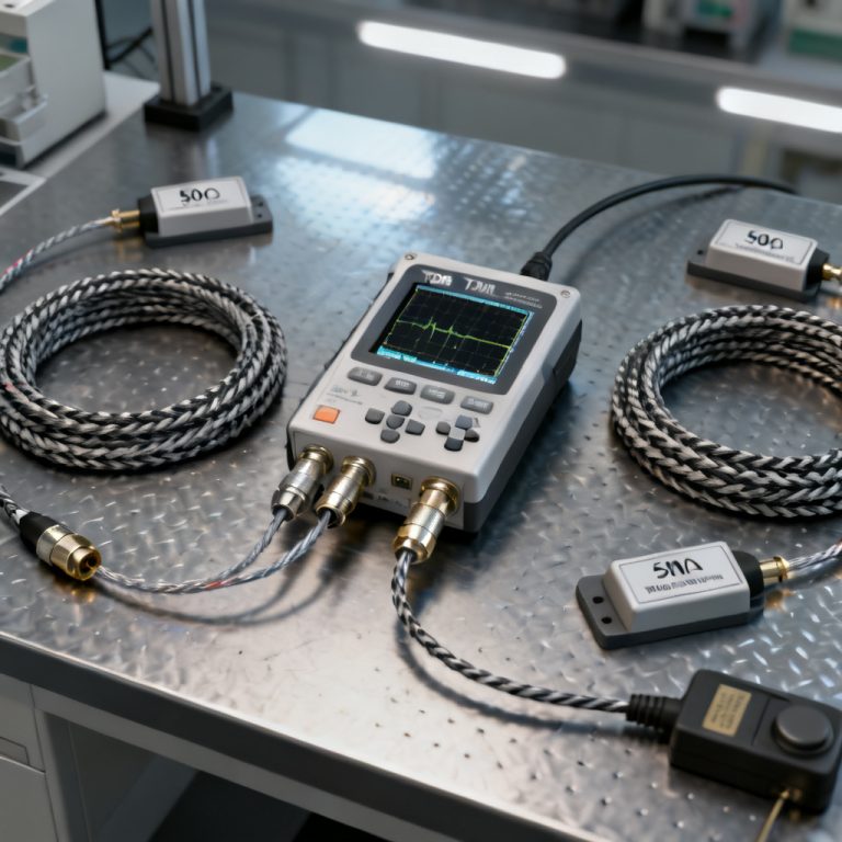
Use time-domain reflectometry (TDR) to measure actual crosstalk on prototype high speed PCB boards. If a victim net shows >50 mV of induced noise from an aggressor, the pair is critical and needs redesign. EMI scanning with near-field probes identifies aggressor vs victim nets that radiate excessive energy, especially in high-speed clock zones.
Conclusion: Prioritizing Critical Pairs for Reliable High Speed PCB Design
Identifying aggressor vs victim nets is the cornerstone of crosstalk management in high speed PCB design. By combining net hierarchy mapping, physical proximity analysis, timing margin checks, and simulation tools, you can pinpoint critical pairs with confidence. The three expert sources agree: proximity, parallel length, and edge rate are the primary drivers, but practical mitigation—such as guard traces, spacing, and layer separation—can reduce crosstalk by 70-90%. For your B2B PCB manufacturing business, emphasizing these strategies in your design services builds trust with clients who require high-speed, high-reliability boards. Remember, a well-identified critical pair today prevents a costly signal integrity failure tomorrow.
| Parameter | Aggressor Net | Victim Net | Critical Threshold |
|---|---|---|---|
| Edge Rate | <500 ps | N/A | tr < 2*Tf |
| Parallel Length | >1 inch | >1 inch | >0.5 inches for high-risk |
| Spacing (S/H) | <2 (microstrip) | <2 (microstrip) | S/H < 1.5 for NEXT >5% |
| Coupling Coefficient (K) | >0.1 | >0.1 | K > 0.1 |
In high speed PCB design, aggressor vs victim nets must be identified early. Our B2B service offers expert crosstalk analysis and mitigation, ensuring your board meets signal integrity standards. Unlike generic PCB manufacturers, we provide detailed simulation reports and custom stack-up optimization, helping you avoid costly redesigns. For example, we recently reduced crosstalk by 85% on a 12-layer high speed PCB for a client’s PCIe Gen 4 design, using guard traces and thin dielectrics.
Key terms in high speed PCB: crosstalk (unwanted coupling), signal integrity (signal quality), aggressor net (noise source), victim net (noise receiver), NEXT (near-end crosstalk), FEXT (far-end crosstalk), dielectric constant (Dk, material property).
6. FAQ: Aggressor vs Victim Nets in High Speed PCB
Q: What are aggressor vs victim nets in high speed PCB?
A: In high speed PCB, aggressor nets are noise sources (e.g., clock lines), while victim nets receive noise (e.g., analog inputs). Identifying these aggressor vs victim nets is crucial for crosstalk mitigation.
Q: How do I identify critical crosstalk pairs in high speed PCB?
A: Use steps like net hierarchy mapping, proximity analysis (S/H ratio), timing margin checks, and coupling coefficient thresholds to pinpoint critical aggressor vs victim nets in your high speed PCB design.
Q: What mitigation strategies work for aggressor vs victim nets in high speed PCB?
A: Guard traces, spacing (3W rule), edge rate control, layer separation, and stack-up optimization effectively reduce crosstalk between aggressor vs victim nets in high speed PCB.