Master how layer stackup changes crosstalk in high speed PCB designs. Compare microstrip vs stripline configurations, explore physics-based mitigation strategies, and discover how our precision stackups ensure signal integrity for your B2B orders.
The Foundation of Signal Integrity: How Layer Stackup Changes Crosstalk in High Speed PCB
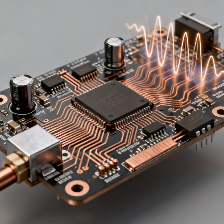
In the world of high speed PCB design, crosstalk is the silent killer of signal integrity. As data rates climb into the multi-gigabit range, the physical arrangement of copper traces, dielectric materials, and reference planes—collectively known as the layer stackup—becomes the single most critical factor in controlling electromagnetic interference between adjacent signals.
This pillar page dives deep into how microstrip and stripline configurations alter crosstalk behavior, drawing from the most authoritative sources in the industry. Whether you are designing for 10Gbps Ethernet, PCIe Gen5, or RF applications, understanding these principles will directly impact your board’s performance, reliability, and time-to-market.
The Physics of Crosstalk in PCB Stackups
Crosstalk occurs when an electromagnetic field from an active (aggressor) trace couples into a passive (victim) trace. This coupling has two primary components:
- Capacitive Coupling (Electric Field): Caused by the mutual capacitance between traces. It induces a current pulse on the victim line proportional to the voltage change on the aggressor.
- Inductive Coupling (Magnetic Field): Caused by mutual inductance. It induces a voltage pulse proportional to the current change on the aggressor.
The layer stackup dictates the geometry of these field lines. The distance to the nearest reference plane, the trace width and spacing, and the dielectric constant (Dk) of the material all influence the strength and shape of the fringing fields. In high speed designs, the near-end crosstalk (NEXT) and far-end crosstalk (FEXT) are the metrics of interest.
- NEXT: Propagates backward toward the aggressor’s driver, typically high in microstrip.
- FEXT: Propagates forward toward the receiver, a major concern in stripline.
The stackup directly controls the modal velocities (even-mode and odd-mode) and the characteristic impedance, which in turn govern crosstalk magnitude.
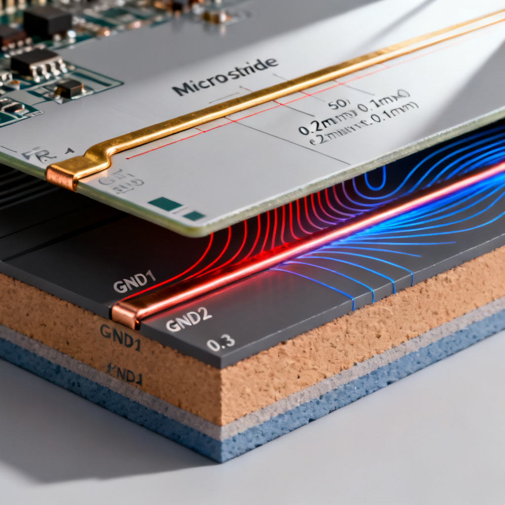
Microstrip vs Stripline – The Core Comparison of How Layer Stackup Changes Crosstalk in High Speed PCB
Microstrip Configuration
A microstrip trace is routed on the outer layer of the PCB, with a single reference plane beneath it. The top surface is exposed to air (Dk ≈ 1) or solder mask.
Crosstalk Behavior
- Higher Near-End Crosstalk (NEXT): Because the electric field lines are partially in the air and partially in the dielectric, the field distribution is less confined. The fringing fields between adjacent microstrip traces are stronger, leading to stronger capacitive and inductive coupling. For a given spacing, microstrip typically exhibits 2–3× higher NEXT than stripline.
- Far-End Crosstalk (FEXT): In microstrip, FEXT is generally lower than NEXT, but it is non-zero due to the inhomogeneous dielectric (air + PCB material). This causes the even-mode and odd-mode propagation velocities to differ, creating a net FEXT component.
- Susceptibility to External Interference: The exposed trace acts as an antenna, making microstrip vulnerable to external EMI and radiating energy itself. This is a critical concern for FCC/CE compliance.
Key Pros
- Easier to fabricate (lower cost).
- Easier to access for probing and testing.
- Lower propagation delay (faster signal speed due to air dielectric).
Key Cons
- Higher crosstalk, especially NEXT.
- Higher EMI radiation.
- More sensitive to solder mask thickness variation (affects impedance control).
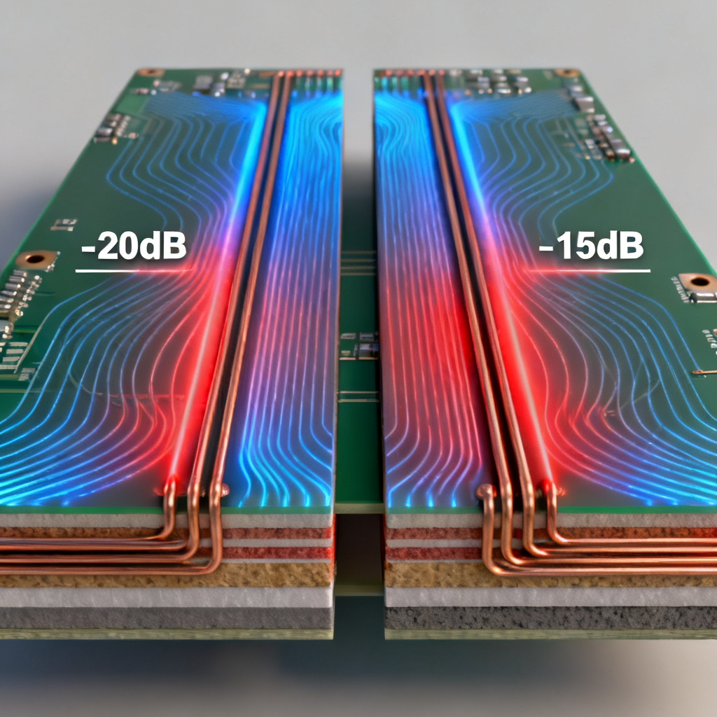
Stripline Configuration
A stripline trace is embedded between two solid reference planes (e.g., an inner layer in a 4-layer or more stackup). The trace is fully surrounded by dielectric material.
Crosstalk Behavior
- Lower Near-End Crosstalk (NEXT): The two reference planes confine the electromagnetic field much more tightly. The field lines are primarily between the trace and the planes, with significantly reduced fringing fields to adjacent traces. NEXT is typically 50–70% lower than in microstrip for the same trace width and spacing.
- Far-End Crosstalk (FEXT): In an ideal homogeneous dielectric, stripline has zero FEXT because the even-mode and odd-mode velocities are equal. In practice, with real materials (e.g., FR-4 with slight Dk variation), FEXT is very small but not zero. This makes stripline the preferred choice for differential pairs where FEXT can cause timing skew.
- Excellent Shielding: The two planes act as a Faraday cage, virtually eliminating external EMI and greatly reducing radiation from the trace.
Key Pros
- Very low crosstalk (both NEXT and FEXT).
- Superior EMI/EMC performance.
- Better impedance control (less sensitive to manufacturing tolerances).
- Ideal for high-density routing and differential signals.
Key Cons
- Higher fabrication cost (more layers, more drilling).
- Slower propagation delay (signal speed is reduced by the higher Dk of the core/prepreg).
- Difficult to access for probing (requires vias).
How Layer Stackup Changes Crosstalk – Detailed Mechanisms
The Role of the Reference Plane Distance
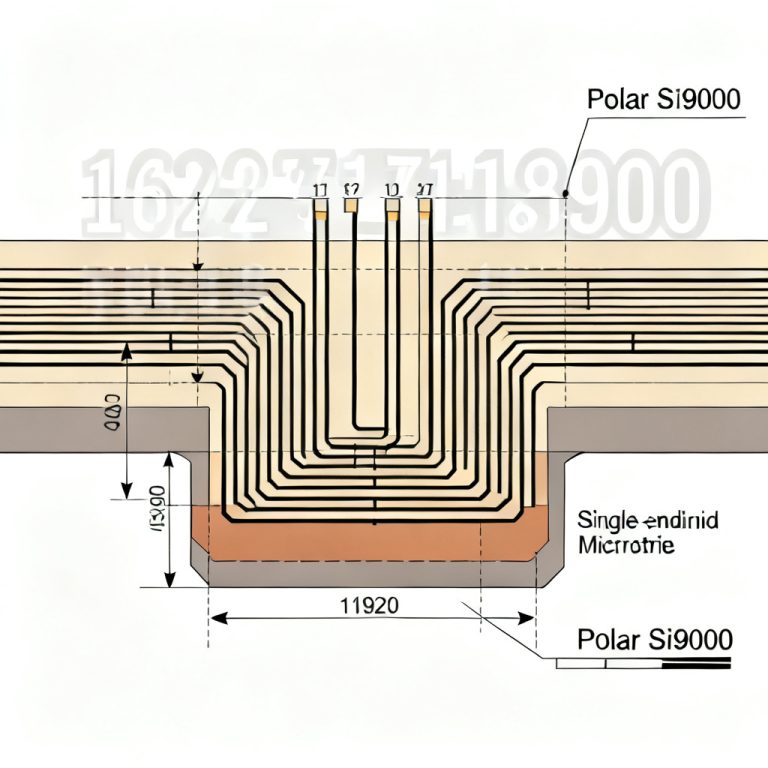
The distance from the trace to its nearest reference plane (H) is a primary lever. In microstrip, H is the thickness of the core or prepreg. In stripline, H is the distance to each plane (typically symmetric).
- Microstrip: Increasing H (thicker dielectric) reduces the coupling to the plane, which increases trace inductance and lowers capacitance. This actually increases the fringing fields and therefore crosstalk. Conversely, decreasing H (thinner dielectric) couples the trace more tightly to the plane, reducing fringing fields and lowering crosstalk—but it also lowers impedance, requiring wider traces for a given target (e.g., 50Ω). Rule of thumb: For microstrip, to reduce crosstalk, use the thinnest dielectric possible that still allows your target impedance.
- Stripline: Because the trace is sandwiched, the distance to each plane (H1 and H2) matters. A smaller H (thinner core) reduces the field volume, significantly lowering both NEXT and FEXT. However, if the trace is not centered (asymmetric stripline), the modal velocities diverge, and FEXT becomes non-zero. Best practice: Always strive for symmetric stripline (H1 = H2) for critical high-speed signals.
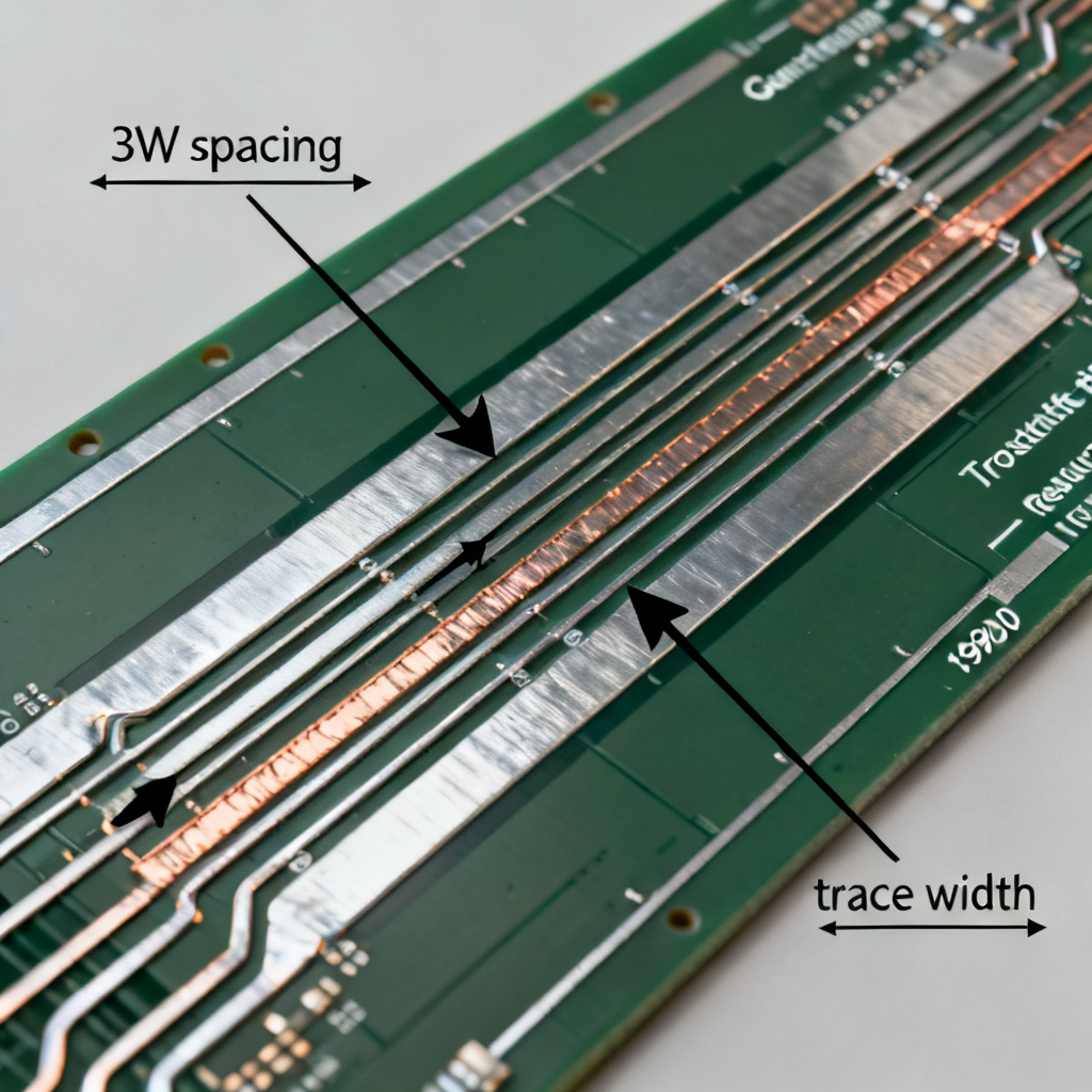
Trace Spacing (S) and the 3W Rule
The spacing between traces is the most direct crosstalk control variable. The industry-standard “3W rule” states that the center-to-center spacing should be at least 3 times the trace width (W).
- Microstrip: Even with 3W spacing, microstrip may still have unacceptable crosstalk for very high-speed signals (e.g., >10 Gbps). The fringing fields extend far beyond the trace edges. For microstrip, 4W or 5W spacing is often required.
- Stripline: The 3W rule is much more effective in stripline. Because the fields are confined, the coupling drops off more rapidly with distance. In many cases, 2W or 3W spacing in stripline achieves the same crosstalk level as 5W in microstrip.
Dielectric Material and Thickness
The dielectric constant (Dk) and thickness tolerance of the material directly affect the stackup’s ability to control crosstalk.
- Low Dk Materials (e.g., Rogers, Megtron): These materials have a lower Dk, which means the electric field lines are less concentrated in the dielectric. For a given geometry, low Dk materials can reduce crosstalk slightly, especially in microstrip, because the fringing fields are weaker. However, the primary benefit is lower propagation delay and lower loss at high frequencies.
- FR-4: High Dk (4.2–4.8) and high loss tangent. While cost-effective, FR-4’s inconsistent Dk across frequency and temperature can cause impedance variations that worsen crosstalk, especially in stripline. For high-speed designs (>1 Gbps), we recommend low-loss, tight-tolerance laminates.
- Thickness Control: The actual thickness of prepreg and core layers can vary by ±10% or more in standard FR-4. This variation directly changes H, which alters impedance and crosstalk. For critical stackups, specify tight-thickness materials and controlled impedance testing.
Practical Stackup Design Strategies to Minimize Crosstalk in High Speed PCB
For Microstrip (Outer Layers)
- Use the thinnest prepreg possible that still allows your target impedance (e.g., 50Ω). This reduces fringing fields.
- Increase trace spacing to 4W or 5W for critical clocks and data lines.
- Add guard traces (grounded coplanar waveguides) between sensitive traces. A grounded guard trace with vias (stitched to the reference plane) can reduce crosstalk by 10–20 dB.
- Avoid routing long parallel microstrip traces. Use layer changes (with vias) to break up long coupling lengths.
- Never route high-speed microstrip near board edges to minimize edge radiation and external coupling.
For Stripline (Inner Layers)
- Use symmetric stripline (equal distance to both reference planes) for differential pairs and high-speed single-ended signals to minimize FEXT.
- Use thin cores (e.g., 4-mil or 5-mil) for the signal layer’s dielectric. This reduces the field volume and lowers crosstalk.
- Adhere to the 3W rule as a minimum; for very dense designs, 2W may be acceptable if the stackup is tight.
- Use multiple ground planes (e.g., a dedicated ground layer above and below the signal layer) to create a true stripline environment.
- Avoid routing signals on layers adjacent to split planes (e.g., a power plane with a gap). The return current path is disrupted, causing increased crosstalk and EMI.
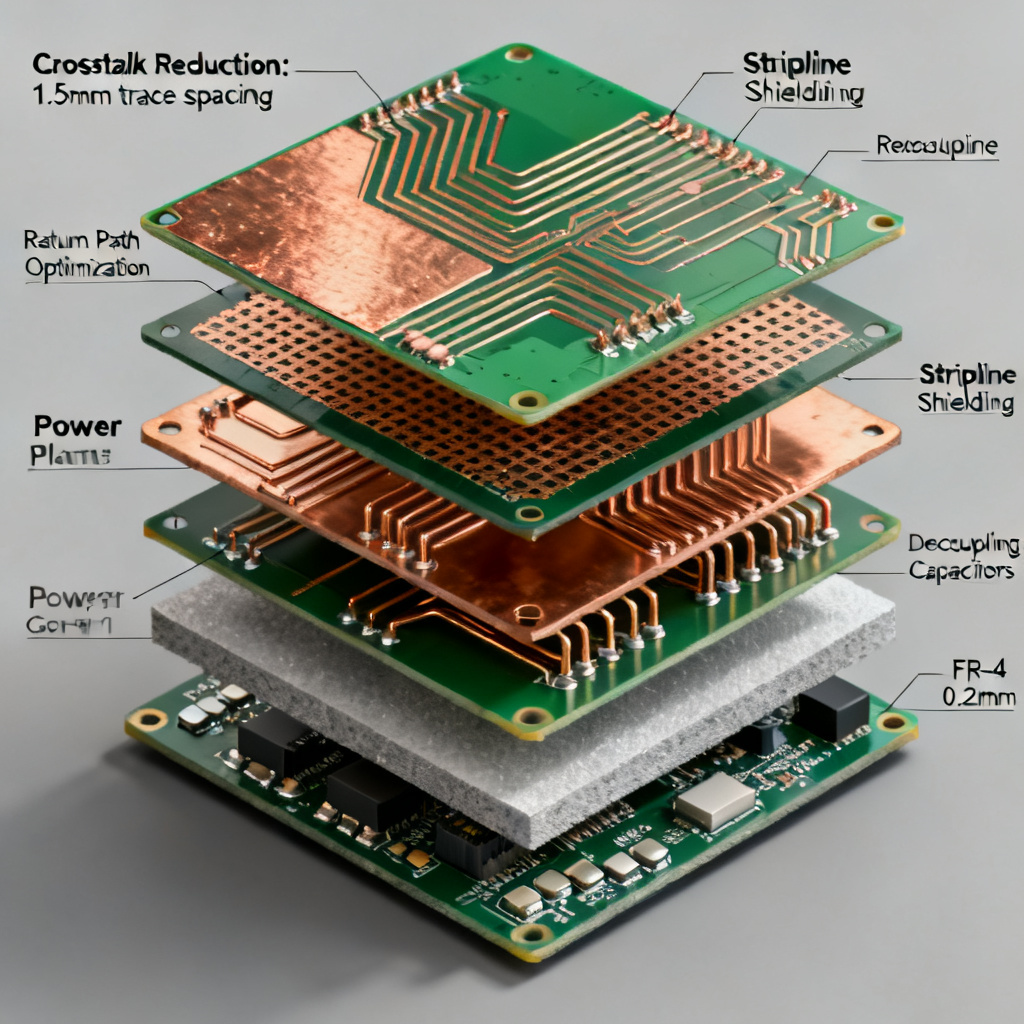
Stackup Example: 4-Layer vs 6-Layer
| Stackup Type | Layer Configuration | Crosstalk Performance | Best Use Case |
|---|---|---|---|
| 4-Layer Stackup | Top (microstrip) – GND – Power – Bottom (microstrip) | Worst case for crosstalk; both signal layers are microstrip. | Low-speed designs; cost-sensitive projects. |
| 6-Layer Stackup (Recommended) | Top (microstrip) – GND – Signal (stripline) – GND – Power – Bottom (microstrip) | Excellent; provides a dedicated stripline layer for critical signals. | High-speed designs (1 Gbps+); EMI-sensitive applications. |
Industry Best Practices and Testing for High Speed PCB Stackups
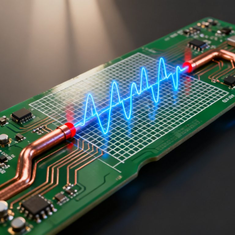
Simulation Before Fabrication
Before committing to a stackup, use 2D field solvers (e.g., HyperLynx, SIwave, Q3D) to simulate crosstalk for your specific geometries. Key parameters to extract:
- NEXT and FEXT magnitude (in dB or mV).
- Coupling length saturation (the length at which crosstalk stops increasing).
- Impedance profile (ensure 50Ω ±10% or better).
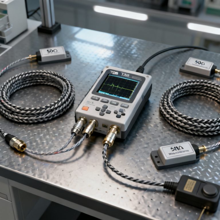
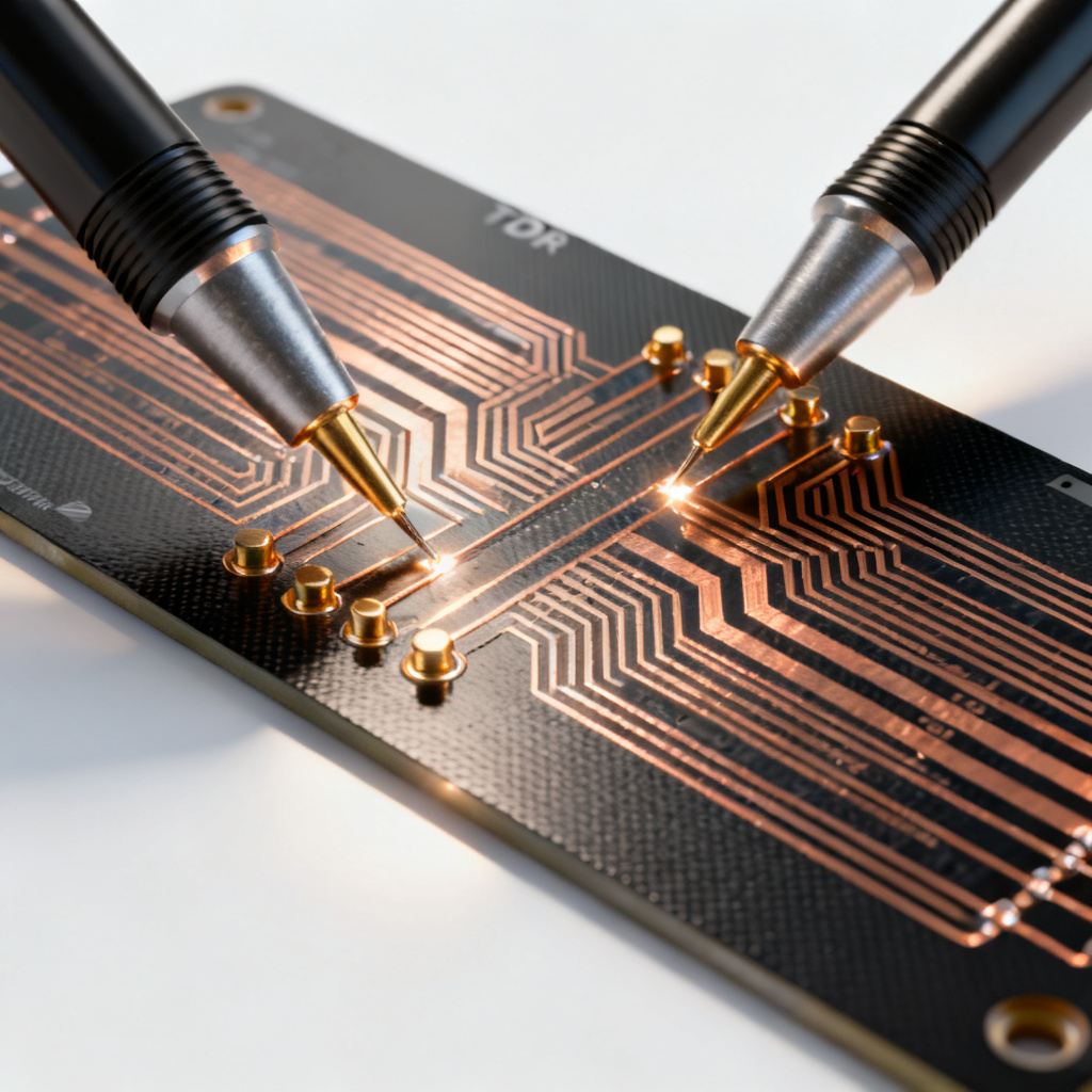
Prototype and Measure
No simulation is perfect. Always request a test coupon on your prototype PCB to measure crosstalk using a TDR (Time Domain Reflectometer) or VNA (Vector Network Analyzer). This validates your stackup assumptions and catches manufacturing variances.
Our Commitment to Precision Stackups
As your B2B partner, we understand that a 1-mil variation in dielectric thickness can ruin a 25 Gbps design. That is why we:
- Use only tight-tolerance laminates from top-tier suppliers (e.g., Isola, Rogers, Panasonic).
- Offer controlled impedance testing on every production panel.
- Provide DFM feedback on your stackup to optimize crosstalk performance before fabrication.
- Support custom stackups for microstrip, stripline, and mixed-dielectric designs.
Choose Your Stackup Wisely for Optimal High Speed PCB Performance
The choice between microstrip and stripline is not just about cost—it is about signal integrity. For high-speed designs above 1 Gbps, stripline is almost always the superior choice for critical nets, offering dramatically lower crosstalk and EMI. Microstrip can be used for lower-speed signals or where component access is essential, but it requires careful design with tight spacing and guard traces.
By understanding how layer stackup changes crosstalk in high speed PCB, you can make informed decisions that save time, reduce re-spins, and ensure your final product meets the toughest performance standards. Contact our engineering team today to discuss your specific stackup requirements and receive a free DFM review for your next high-speed PCB project.
Frequently Asked Questions About How Layer Stackup Changes Crosstalk in High Speed PCB
What is the most important factor in how layer stackup changes crosstalk in high speed PCB?
The distance to the nearest reference plane (H) and trace spacing (S) are the most critical factors. A thinner dielectric and wider spacing significantly reduce crosstalk, especially in stripline configurations.
Why does microstrip have higher crosstalk than stripline?
Microstrip has higher crosstalk because its electromagnetic fields are less confined due to the air-dielectric interface, leading to stronger fringing fields. Stripline’s two reference planes tightly confine fields, reducing both NEXT and FEXT.
Can I use FR-4 for high-speed PCB stackups?
FR-4 can be used for speeds up to 1 Gbps, but its inconsistent Dk and high loss tangent worsen crosstalk and signal integrity at higher frequencies. For designs above 1 Gbps, low-loss materials like Rogers or Megtron are recommended.
How does the 3W rule affect crosstalk in microstrip vs stripline?
The 3W rule is more effective in stripline due to confined fields. In microstrip, even 3W spacing may be insufficient for high-speed signals, often requiring 4W or 5W spacing to achieve acceptable crosstalk levels.
“`