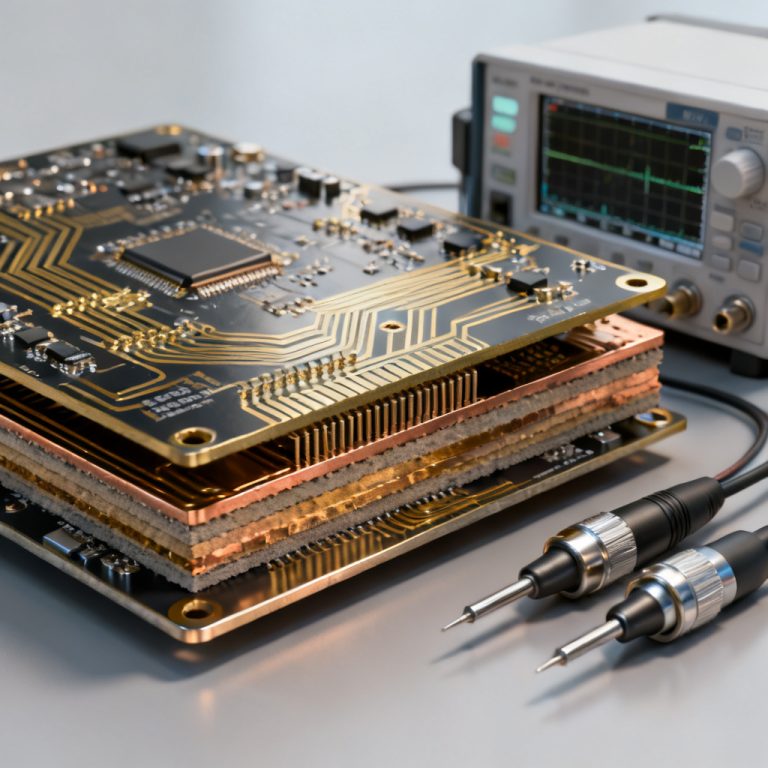
Automated crosstalk checks in high speed PCB design rule checking is essential for reliable signal integrity in modern electronics. This guide provides a complete framework for integrating automated crosstalk analysis into your design workflow, drawing from the most authoritative industry sources.

Understanding Crosstalk Fundamentals for High Speed PCB Design Rule Checking
What Is Crosstalk and Why It Matters in High Speed PCB Design Rule Checking
Crosstalk is unwanted electromagnetic coupling between adjacent traces in a high speed PCB. It occurs when an aggressor signal induces voltage or current in a victim net, causing false switching or timing violations. Automated crosstalk checks in high speed PCB design rule checking detect these issues early.
Key types include capacitive coupling (electric field), inductive coupling (magnetic field), and forward/backward crosstalk. Backward crosstalk is more problematic in microstrip topologies.
Key Parameters Influencing Crosstalk in High Speed PCB Design Rule Checking
To automate crosstalk checks effectively, understand these variables:
- Trace spacing: Closer spacing increases coupling. Industry standards recommend 3W for microstrip, 5W for stripline.
- Dielectric height (H): Smaller H increases coupling.
- Trace length: Longer parallel runs amplify crosstalk.
- Signal rise time (Tr): Faster edges generate higher-frequency harmonics.
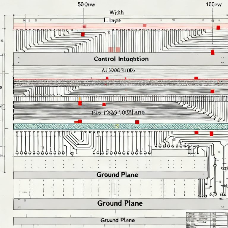
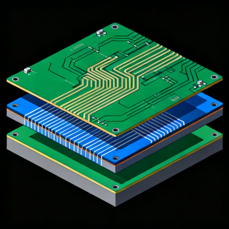
- Layer stackup: Stripline offers lower crosstalk than microstrip.
- Termination: Improper termination worsens crosstalk.
Why Automation Is Essential for High Speed PCB Design Rule Checking
Manual crosstalk checking is impractical for dense boards. Automation provides speed, consistency, accuracy, and iterative optimization. Modern EDA tools integrate real-time DRC for crosstalk.
Setting Up Automated Crosstalk Design Rules for High Speed PCB Design Rule Checking
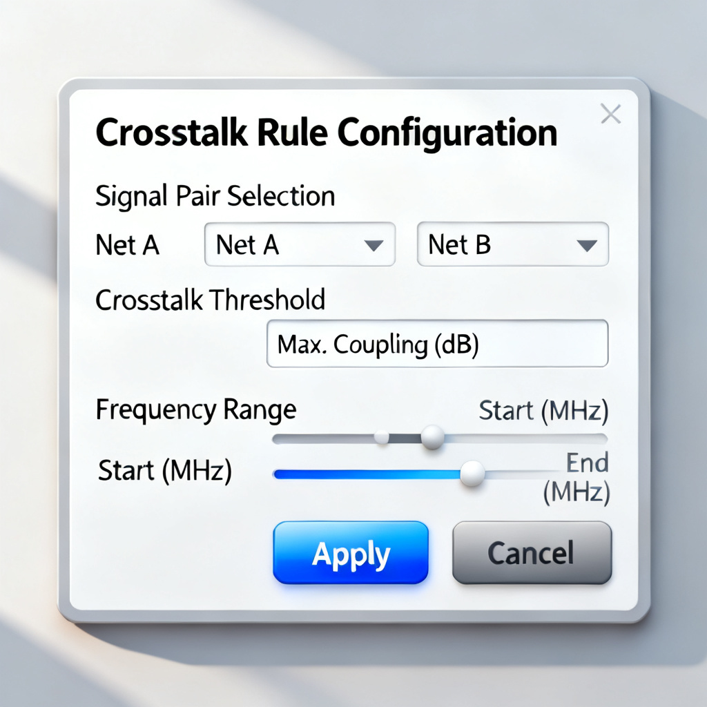
Step 1: Define Crosstalk-Specific DRC Rules for High Speed PCB Design Rule Checking
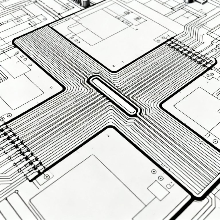
Create custom DRC rules beyond standard spacing. Key rules include parallelism length, coupling threshold, aggressor-victim classification, and spatial proximity. Example from Altium: Parallel Segment rule with max parallel length = 50mm, min spacing = 0.2mm, applied to high-speed net class.
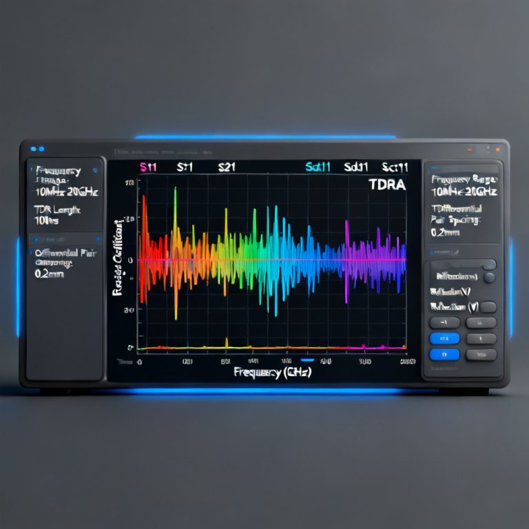
Step 2: Integrate SI Simulation for Pre-Layout Crosstalk Estimation
Use pre-layout SI tools like Cadence Sigrity or Altium PDN Analyzer to estimate coupling. Output a coupling coefficient map for critical net identification. Sierra Circuits uses field solvers like Ansys Q3D to extract RLGC parameters.
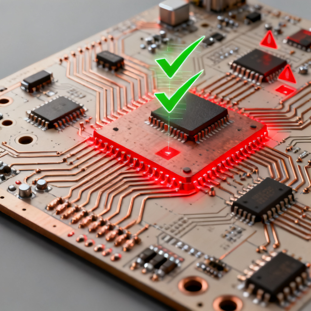
Step 3: Implement Real-Time DRC During Layout
Enable real-time DRC in EDA tools. Cadence Allegro uses Constraint Manager with Crosstalk tab. Altium Designer uses PCB Rules and Constraints Editor. OrCAD uses Electrical Constraint Set. Share your DRC rule file with fabrication partners.
Step 4: Post-Layout Automated Crosstalk Verification
Run batch-mode DRC scan after routing. Cadence Sigrity generates coupling reports. Altium exports violation reports. Sierra Circuits uses HyperLynx for full board simulation.
Advanced Automation Techniques for High Speed PCB Design Rule Checking
Automatic Guard Trace Insertion
Some EDA tools auto-insert grounded guard traces. Altium uses Via Stitching and Guard Trace rules. Cadence uses Auto Guard under Route menu. Workflow: identify nets with >0.1 coupling, run script, re-run DRC.
Automated Layer Assignment Based on Crosstalk Sensitivity
Use scripted DRC to move high-risk nets to stripline layers. Cadence Skill scripts or Altium DelphiScript automate net class changes. Example: move nets with coupling >0.15 to Layer 3.
Integration with PCB Fabrication DFM
Share automated crosstalk DRC results with manufacturers. Sierra Circuits provides free DFM crosstalk check. Export violations as CSV for cross-verification.
Case Studies and Best Practices for High Speed PCB Design Rule Checking
Case Study 1: Cadence – 16-Layer Server Board
Challenge: 100+ high-speed nets (PCIe Gen4, DDR4) with intermittent failures. Solution: Sigrity automated crosstalk DRC with coupling coefficient limit 0.05. Real-time DRC flagged 23 violations. Result: 95% first-pass success.
Case Study 2: Altium – 4-Layer IoT Module
Challenge: Tight 0.15mm spacing for USB 3.0. Solution: Parallelism rule with max parallel length 30mm. Automated DRC flagged 12 violations in 5 minutes. Result: Design cycle reduced from 3 to 2 weeks.
Case Study 3: Sierra Circuits – 5G Antenna Board
Challenge: 28 GHz microstrip with severe crosstalk. Solution: Pre-layout SI simulation set 0.08 coupling limit. Automated DRC enforced 5W spacing. Result: Coupling below 0.05.
Best Practices for B2B PCB Buyers
- Specify crosstalk DRC in your RFQ.
- Request a DRC report before production.
- Use a unified rule file with manufacturer.
- Invest in SI simulation tools for 10 Gbps+ designs.
Step-by-Step Automation Workflow for High Speed PCB Design Rule Checking
Step 1: Pre-Layout – Define Net Classes and Coupling Limits
Identify critical nets. Set coupling coefficient limit (e.g., 0.1 for <1 Gbps, 0.05 for >10 Gbps). Create crosstalk rule set.
Step 2: Layout – Enable Real-Time DRC
Activate high-speed DRC rules. Route critical nets first. Use auto guard trace if coupling exceeds limit.
Step 3: Post-Layout – Run Batch DRC and SI Simulation
Run full board DRC. Export violation report. Simulate top 10 critical net pairs.
Step 4: Mitigation – Apply Automated Fixes
Increase spacing to 5W for spacing violations. Add serpentine routing for length violations. Move net to different layer or add guard trace for coupling violations.
Step 5: Verification – Final DRC and DFM Check
Re-run DRC. Send Gerber files and DRC report to manufacturer for DFM crosstalk check.
Frequently Asked Questions About High Speed PCB Design Rule Checking for Crosstalk
What is the 3W rule in high speed PCB design rule checking for crosstalk?
How do I automate crosstalk checks in Altium for high speed PCB design rule checking?
What tools support automated crosstalk analysis for high speed PCB design rule checking?
Key Terminology for High Speed PCB Design Rule Checking
| Parameter | Description | Typical Value |
|---|---|---|
| Coupling Coefficient | Ratio of induced voltage to aggressor voltage | <0.1 for <1 Gbps, <0.05 for >10 Gbps |
| Parallelism Length | Maximum allowed parallel run between nets | 30–50 mm for high-speed nets |
| Trace Spacing | Edge-to-edge distance between traces | 3W (microstrip), 5W (stripline) |
| Guard Trace Width | Width of grounded guard trace | 2x signal trace width |
Comparison: Automated vs Manual Crosstalk Checks in High Speed PCB Design Rule Checking
| Aspect | Automated DRC | Manual Checking |
|---|---|---|
| Speed | Full board scan in minutes | Hours to days |
| Accuracy | Detects subtle violations | Prone to human error |
| Consistency | Same rules applied globally | Varies by engineer |
| Iterative Optimization | Rapid what-if analysis | Time-consuming |