This practical guide explains how to use TDR/TDT to measure crosstalk in high speed PCB designs. Mastering this technique is essential for signal integrity engineers working on advanced digital systems.
In high-speed PCB design, crosstalk is a critical signal integrity issue that can degrade performance and cause system failures. Time Domain Reflectometry (TDR) and Time Domain Transmission (TDT) provide precise measurements to identify and quantify crosstalk coupling between traces. This comprehensive guide covers the physics, equipment, calibration, measurement methodology, and interpretation of results for using TDR/TDT to measure crosstalk in high speed PCB.
Fundamentals of TDR/TDT for Crosstalk Measurement in High Speed PCB
Why TDR/TDT for Crosstalk Measurement in High Speed PCB?
Using TDR/TDT to measure crosstalk in high speed PCB offers distinct advantages over frequency-domain methods. Traditional VNA measurements require complex calibration and often fail to isolate weak coupling in dense multi-layer PCB stacks. TDR/TDT provides superior time-domain resolution, allowing engineers to pinpoint the exact location and magnitude of coupling along a trace.
When you use TDR/TDT to measure crosstalk in high speed PCB, you gain the ability to distinguish between near-end crosstalk (NEXT) and far-end crosstalk (FEXT). This distinction is crucial for optimizing layout and material selection in high speed PCB manufacturing.
The Physics of Crosstalk in TDR/TDT
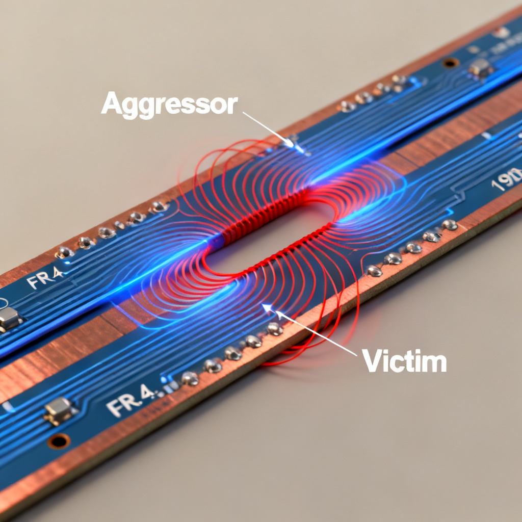
When a step pulse propagates down an aggressor trace, it generates both electric (capacitive) and magnetic (inductive) fields. These fields couple into adjacent victim traces. The crosstalk voltage measured by TDT is the superposition of forward crosstalk (FEXT) and backward crosstalk (NEXT). Using TDR/TDT to measure crosstalk in high speed PCB reveals the polarity and timing of these components, enabling engineers to distinguish between capacitive and inductive coupling mechanisms.
In microstrip traces, FEXT dominates due to inhomogeneous dielectric, while in stripline traces, NEXT dominates due to homogeneous dielectric. Understanding these physics is fundamental to using TDR/TDT to measure crosstalk in high speed PCB effectively.
Equipment Setup and Calibration for TDR/TDT Crosstalk Measurement
Essential Equipment Components
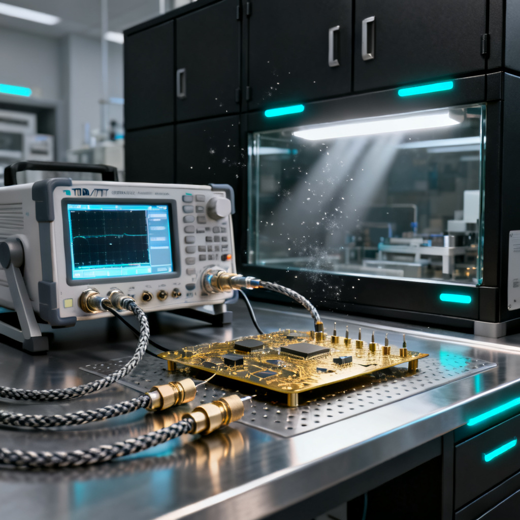
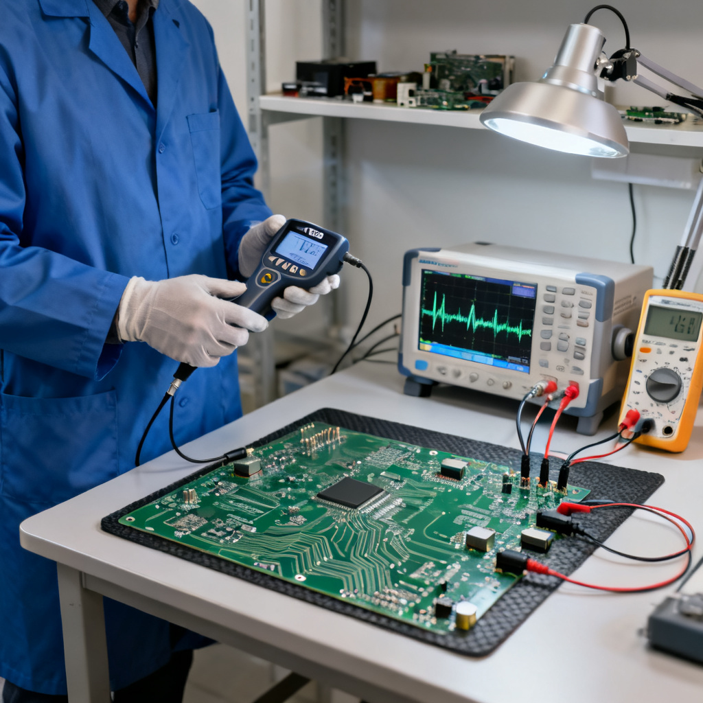
To use TDR/TDT to measure crosstalk in high speed PCB, you need specific equipment. A TDR/TDT sampling oscilloscope with bandwidth ≥ 20 GHz (50 GHz preferred for sub-20 ps rise times) is essential. The pulse generator must have a rise time < 30 ps. Probes and cables must be low-loss and phase-stable. Calibration standards including open, short, load (50 Ω), and through standards are required.
For accurate results when using TDR/TDT to measure crosstalk in high speed PCB, the victim trace must be terminated with its characteristic impedance (Z0) at both ends. If the victim is left open, reflections will distort the TDT waveform.
| Equipment Component | Specification for Crosstalk Measurement in High Speed PCB | Recommended Model |
|---|---|---|
| Sampling Oscilloscope | Bandwidth ≥ 20 GHz | Keysight DCA-X, Tektronix DSA8300 |
| Pulse Generator | Rise time < 30 ps | Picosecond Pulse Labs 4022 |
| Cables | Low-loss, phase-stable | Gore, Huber+Suhner |
| Probes | High-impedance, matched-length | Cascade Microtech Infinity |
Calibration Procedure for TDR/TDT Crosstalk Measurement
Proper calibration is critical when using TDR/TDT to measure crosstalk in high speed PCB. First, allow all equipment to warm up for 30 minutes. Perform oscilloscope self-calibration including deskew and normalization. Measure the incident pulse amplitude and rise time at the probe tip using a 50 Ω through. For de-embedding, use a known open/short on the PCB to remove fixture effects. Finally, connect both aggressor and victim traces to 50 Ω loads and record the noise floor (typically < -60 dB relative to incident pulse).
When using TDR/TDT to measure crosstalk in high speed PCB, de-embedding is recommended but optional. Many modern oscilloscopes have built-in de-embedding algorithms that simplify this process.
Measurement Methodology Using TDR/TDT for High Speed PCB Crosstalk
Performing the TDR Measurement (Reflection Mode)
To use TDR/TDT to measure crosstalk in high speed PCB in reflection mode, connect the TDR pulse generator to the aggressor trace. Set the oscilloscope to display the reflected waveform (TDR mode). Observe the impedance profile. A crosstalk event appears as a small dip (capacitive coupling) or peak (inductive coupling) at the location of the coupling zone. Quantify the peak-to-peak amplitude of the crosstalk-induced reflection and convert to impedance change using: ΔZ = (V_reflected / V_incident) × 50 Ω.
If the crosstalk reflection is buried in noise when using TDR/TDT to measure crosstalk in high speed PCB, increase the number of averages (e.g., 64 or 128) and use a low-pass filter (e.g., 10 GHz bandwidth limit).
Performing the TDT Measurement (Transmission Mode)
To use TDR/TDT to measure crosstalk in high speed PCB in transmission mode, connect the TDR pulse generator to the aggressor trace. Connect the victim trace (far end) to a high-impedance input. Record the transmitted waveform on the victim trace. Forward crosstalk (FEXT) appears as a pulse that arrives at the same time as the aggressor pulse at the far end. Backward crosstalk (NEXT) appears as a pulse that arrives earlier (since it travels backward).
When using TDR/TDT to measure crosstalk in high speed PCB, the polarity of the crosstalk pulse reveals the coupling mechanism: same polarity as aggressor for capacitive coupling; opposite polarity for inductive coupling.
Measuring Differential Crosstalk with TDR/TDT
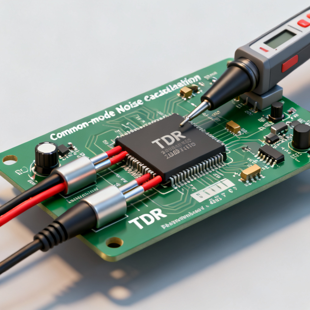
For differential pairs (e.g., USB, PCIe, HDMI), using TDR/TDT to measure crosstalk in high speed PCB requires a specific approach. Connect the TDR pulse to the positive leg of the aggressor pair with the negative leg grounded. Measure TDT on the positive leg of the victim pair. Repeat with the negative leg. Differential crosstalk = (V_TDT_positive – V_TDT_negative) / 2. This eliminates common-mode noise and provides accurate measurement of differential crosstalk in high speed PCB.
Interpreting TDR/TDT Results for High Speed PCB Crosstalk
Reading the TDR/TDT Waveforms
When using TDR/TDT to measure crosstalk in high speed PCB, a clean TDR waveform shows a flat impedance line (e.g., 50 Ω ± 2 Ω) with no dips or peaks. A crosstalk signature appears as a small, localized impedance change (e.g., ±0.5 Ω) at the coupling zone. The TDT waveform shows a pulse with amplitude proportional to coupling strength. Typical acceptable levels for high speed PCB are < -30 dB (1% voltage) for most standards, and < -40 dB for critical links (e.g., 25 Gbps NRZ).
Converting TDT Voltage to Crosstalk Coefficient
To quantify results when using TDR/TDT to measure crosstalk in high speed PCB, use the formula: Crosstalk (dB) = 20 × log10(V_TDT / V_incident). For example, if V_incident = 500 mV and V_TDT = 5 mV, crosstalk = -40 dB. This conversion is essential for comparing results against industry standards and design specifications.
Common Pitfalls in Interpretation
When using TDR/TDT to measure crosstalk in high speed PCB, reflections from vias or connectors can appear as crosstalk events. To distinguish, move the probe to a different victim trace—if the waveform changes, it’s crosstalk. Dielectric loss at high frequencies attenuates the crosstalk pulse, making it appear smaller than at DC. Use low-loss materials (e.g., Rogers, Megtron 6) for accurate high-frequency crosstalk measurement. Edge effects can broaden or split the crosstalk pulse if the aggressor and victim traces are not parallel for their entire length.
Practical Examples of TDR/TDT Crosstalk Measurement in High Speed PCB
Example 1: 10 Gbps PCIe Gen 3 Lane-to-Lane Crosstalk
In this case of using TDR/TDT to measure crosstalk in high speed PCB, microstrip traces on FR4 with 4 mil width, 6 mil spacing, and 4-inch parallel run were tested. TDR showed an impedance dip of 0.8 Ω at the midpoint of the coupling zone. TDT showed a FEXT pulse amplitude of 12 mV (V_incident = 500 mV), resulting in crosstalk of -32 dB. The action taken was to increase spacing to 10 mil and reduce parallel length to 2 inches, which dropped crosstalk to -42 dB.
Example 2: 25 Gbps NRZ (IEEE 802.3bj) Backplane
When using TDR/TDT to measure crosstalk in high speed PCB for this backplane design, stripline traces on Megtron 6 with 8 mil width, 12 mil spacing, and 10-inch run were tested. TDR showed multiple small peaks (inductive coupling) along the entire length. TDT showed a NEXT pulse amplitude of 3 mV (V_incident = 400 mV), resulting in crosstalk of -42 dB. Adding ground stitching vias between aggressor and victim layers reduced crosstalk to -50 dB.
Example 3: DDR4 Memory Bus (1.2 V, 3200 MT/s)
For this application of using TDR/TDT to measure crosstalk in high speed PCB, microstrip traces on FR4 with 5 mil width, 8 mil spacing, and 1.5-inch parallel run were tested. TDR showed a capacitive dip of 0.3 Ω. TDT showed a FEXT pulse amplitude of 8 mV. Routing the victim trace on a different layer with a ground plane between them made crosstalk negligible (< -60 dB).
Advanced Techniques for TDR/TDT Crosstalk Measurement in High Speed PCB
Using Differential TDR/TDT for High-Speed Serial Links
For serial standards (e.g., SATA, SAS, USB 3.0, 10GBASE-KR), using TDR/TDT to measure crosstalk in high speed PCB requires a four-port TDR setup (two aggressors, two victims). The measurement procedure is identical but yields differential crosstalk coefficients. This approach is essential for validating differential signal integrity in modern high speed PCB designs.
Time-Domain vs. Frequency-Domain Correlation
If you have a VNA, you can convert TDT data to frequency domain via FFT when using TDR/TDT to measure crosstalk in high speed PCB. This allows direct comparison with S-parameters (e.g., S31, S41). TDT crosstalk at low frequencies (e.g., < 1 GHz) correlates with capacitive coupling; at high frequencies (> 5 GHz), inductive coupling dominates.
Reducing Measurement Noise
To improve accuracy when using TDR/TDT to measure crosstalk in high speed PCB, use 256 averages for clean TDT waveforms. Place the PCB in a Faraday cage (e.g., copper tape box) to eliminate ambient EMI. Keep lab temperature stable (±2°C) since FR4’s dielectric constant (Dk) changes with temperature (≈ 0.1% per °C).
De-embedding Fixtures and Test Structures
If using a test coupon (e.g., IPC-2141A) when using TDR/TDT to measure crosstalk in high speed PCB, de-embed the launch structures (SMA connectors, via transitions) using a TRL calibration. This isolates the crosstalk of the trace itself from the fixture, providing more accurate results.
Troubleshooting TDR/TDT Crosstalk Measurement in High Speed PCB
Why is my TDT waveform showing a negative pulse?
Negative polarity indicates inductive coupling (mutual inductance) dominates. This is common in stripline where the dielectric is homogeneous. Positive pulse indicates capacitive coupling dominance (common in microstrip). Understanding this polarity is key when using TDR/TDT to measure crosstalk in high speed PCB.
My TDR shows a large impedance dip but TDT shows negligible crosstalk. Why?
The impedance dip may be due to a physical discontinuity (e.g., a via stub) rather than crosstalk. Check by moving the victim trace—if the dip remains, it’s a discontinuity, not coupling. This is a common pitfall when using TDR/TDT to measure crosstalk in high speed PCB.
How do I measure crosstalk on a multi-layer board with buried traces?
You must expose the via pads for both aggressor and victim. Use a micro-probe station with fine-pitch probes (e.g., 100 μm pitch). Alternatively, use a VNA with a four-port test fixture. This approach is necessary when using TDR/TDT to measure crosstalk in high speed PCB with complex layer stacks.
What is the minimum detectable crosstalk with TDT?
With a 50 GHz oscilloscope and 256 averages, you can reliably measure crosstalk down to -60 dB (1 mV on a 1 V incident pulse). Below that, thermal noise and jitter dominate. This sensitivity makes using TDR/TDT to measure crosstalk in high speed PCB highly effective for most applications.
Integrating TDR/TDT into Your High Speed PCB Design Flow
Using TDR/TDT to measure crosstalk in high speed PCB is not just a lab exercise—it is a critical step in validating your design before production. By following this guide, you can identify the exact location and magnitude of coupling, distinguish between capacitive and inductive mechanisms, quantify crosstalk in dB relative to your system’s margin, and make data-driven decisions on spacing, layer stackup, and material selection.
At [Your Company Name], we integrate TDR/TDT validation into every high speed PCB prototype. Our in-house 50 GHz sampling oscilloscopes and advanced de-embedding algorithms ensure your design meets signal integrity targets before we ship. Whether you need a 4-layer prototype or a 32-layer backplane, we deliver crosstalk-optimized boards with guaranteed performance. Contact us today for a free TDR/TDT analysis of your high speed PCB layout.
Frequently Asked Questions About Using TDR/TDT to Measure Crosstalk in High Speed PCB
What is the difference between TDR and TDT when measuring crosstalk in high speed PCB?
TDR (Time Domain Reflectometry) measures reflected voltage on the aggressor trace to identify where crosstalk coupling occurs. TDT (Time Domain Transmission) measures transmitted energy on the victim trace to quantify how much crosstalk is induced. Both are essential for comprehensive crosstalk analysis in high speed PCB.
What equipment do I need to use TDR/TDT to measure crosstalk in high speed PCB?
You need a TDR/TDT sampling oscilloscope with bandwidth ≥ 20 GHz, a pulse generator with rise time < 30 ps, low-loss phase-stable cables, high-impedance probes, and calibration standards (open, short, load, through). Proper equipment ensures accurate crosstalk measurement in high speed PCB.
How do I calibrate the setup for TDR/TDT crosstalk measurement in high speed PCB?
Warm up equipment for 30 minutes, perform oscilloscope self-calibration, measure incident pulse at probe tip, perform de-embedding using known open/short on PCB, and record noise floor with both traces terminated to 50 Ω. Proper calibration is critical for accurate results when measuring crosstalk in high speed PCB.
What are acceptable crosstalk levels in high speed PCB?
Typical acceptable levels are < -30 dB (1% voltage) for most high-speed standards and < -40 dB for critical links like 25 Gbps NRZ. These levels ensure reliable signal integrity when using TDR/TDT to measure crosstalk in high speed PCB designs.
How can I reduce crosstalk in high speed PCB based on TDR/TDT measurements?
Based on TDR/TDT results, you can increase trace spacing, reduce parallel run length, add ground stitching vias, use low-loss materials, route victim traces on different layers with ground planes between them, and optimize layer stackup. These techniques are validated when you use TDR/TDT to measure crosstalk in high speed PCB.
Can TDR/TDT measure differential crosstalk in high speed PCB?
Yes, for differential pairs (e.g., USB, PCIe, HDMI), connect the TDR pulse to the positive leg of the aggressor pair, measure TDT on both legs of the victim pair, and calculate differential crosstalk as (V_TDT_positive – V_TDT_negative) / 2. This eliminates common-mode noise when using TDR/TDT to measure crosstalk in high speed PCB.
Industry Terminology for TDR/TDT Crosstalk Measurement in High Speed PCB
Aggressor Trace: The trace carrying the high-speed signal that induces crosstalk into adjacent traces. In TDR/TDT measurement, this is the trace where the pulse is launched.
Victim Trace: The trace that receives unwanted coupled energy from the aggressor trace. This trace is monitored during TDT measurement.
Forward Crosstalk (FEXT): Crosstalk that propagates in the same direction as the aggressor pulse. Dominant in microstrip traces due to inhomogeneous dielectric.
Backward Crosstalk (NEXT): Crosstalk that propagates in the opposite direction. Dominant in stripline traces due to homogeneous dielectric.
Characteristic Impedance (Z0): The impedance a transmission line presents to a propagating signal. Typically 50 Ω for single-ended traces in high speed PCB.
De-embedding: A calibration technique that removes the effects of test fixtures and probes from measurement results, providing more accurate crosstalk data.