In high-speed PCB design, multiple reflections in transmission line directly cause ringing and extended settling time, degrading signal integrity. This pillar content explores the physics, impact, and mitigation of these reflections for reliable high-speed PCB performance.
Physics of Multiple Reflections in Transmission Line
Reflection Coefficient and Impedance Mismatch
When a signal encounters an impedance change, a portion of the incident voltage is reflected back toward the source. The reflection coefficient (Γ) at a boundary is defined as:
Γ = (Z_L – Z_0) / (Z_L + Z_0)
where Z_0 is the characteristic impedance of the transmission line (typically 50Ω in high-speed PCB designs) and Z_L is the load impedance. A mismatch between Z_0 and Z_L (or source impedance Z_S) creates a non-zero reflection coefficient. For example, if Z_L is open (infinite), Γ = +1 (full positive reflection); if shorted (0Ω), Γ = -1 (full negative reflection). In practice, even small mismatches (e.g., ±10% due to manufacturing tolerances or via stubs) generate reflections that degrade signal quality.
The Mechanism of Multiple Reflections in Transmission Line
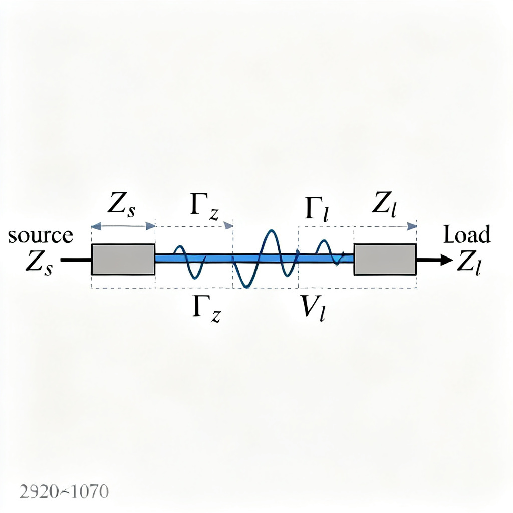
Multiple reflections in transmission line occur when the signal reflects back and forth between discontinuities, typically between the source and load ends of a transmission line. Consider a simple scenario: a driver with source impedance Z_S, a line of length L with characteristic impedance Z_0, and a receiver with load impedance Z_L. When the driver launches a step signal, the initial voltage at the source is divided between Z_S and Z_0. This wave travels to the load, reflects based on Γ_L, travels back to the source, reflects again based on Γ_S, and so on. Each round trip adds a delayed, attenuated component to the signal at the load.
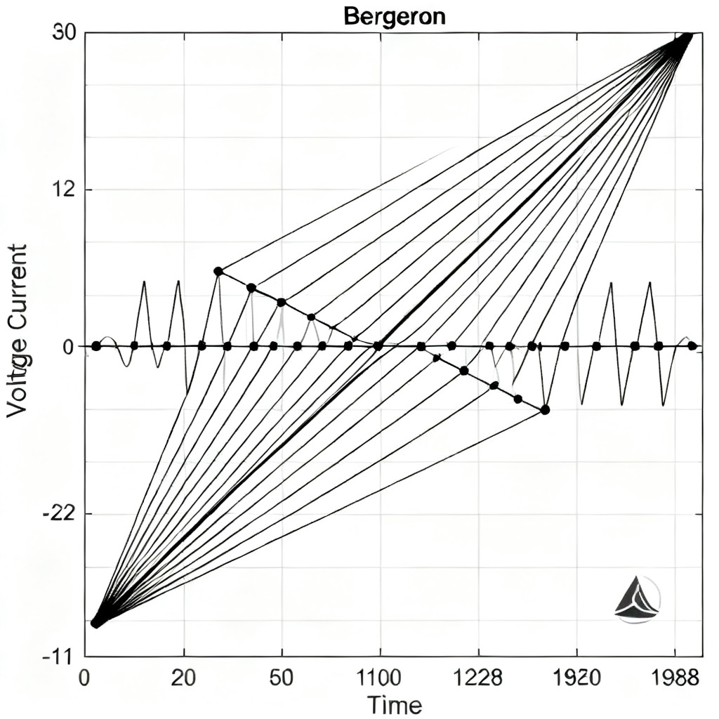
This iterative process creates a lattice diagram (Bergeron plot) that visualizes the time-domain evolution of reflections. For instance, with Z_S = 10Ω, Z_0 = 50Ω, and Z_L = 1MΩ (high impedance), the initial reflection at the load is nearly full positive (Γ ≈ 0.96), causing a voltage overshoot. The reflected wave then sees a large mismatch at the source (Γ_S ≈ -0.67), generating a negative reflection. This back-and-forth continues, producing a series of step-like changes that gradually converge to the steady-state voltage.
Key Factors Influencing Reflection Magnitude and Duration
- Impedance mismatch magnitude: Larger mismatches (e.g., open or short) produce stronger reflections.
- Line length: Longer lines increase the round-trip delay, making reflections more visible at lower frequencies.
- Rise time: Faster rise times (common in high-speed signals like DDR5 or PCIe Gen5) excite higher-frequency components, making reflections more pronounced.
- Number of discontinuities: Multiple vias, connectors, or stubs create complex reflection patterns.
How Multiple Reflections in Transmission Line Create Ringing
Ringing as a Manifestation of Reflected Energy
Ringing is the oscillatory transient response observed at the receiver (or any point along the line) after the initial signal edge. It arises from constructive and destructive interference of multiple reflections in transmission line. When the round-trip delay (2 × propagation delay per unit length × L) is comparable to or longer than the signal rise time, the reflections do not fully settle before the next reflection arrives, leading to sustained oscillations.
For example, in a mismatched line with Z_S < Z_0 < Z_L, the first reflection at the load is positive (overshoot), the second reflection (from the source) is negative (undershoot), and subsequent reflections alternate in polarity but with diminishing amplitude. The resulting waveform at the load shows a damped sinusoidal ringing, with frequency approximately equal to:
f_ringing ≈ 1 / (2 × t_pd × L)
where t_pd is the propagation delay per unit length (e.g., ~6 ps/mm for FR4). This frequency can be in the hundreds of megahertz to low gigahertz range for typical PCB traces.
The Role of Damping Factor
The damping of ringing depends on the reflection coefficients and line losses. In an ideal lossless line with perfect mismatches (Γ = ±1), ringing would persist indefinitely. In practice, dielectric losses (tan δ) and conductor losses (skin effect) attenuate higher-frequency components, reducing ringing amplitude over time. However, for high-speed designs with low-loss materials (e.g., Rogers 4350B), damping is minimal, and ringing can last for several nanoseconds—potentially exceeding the bit period in multi-gigabit systems.
Impact on Signal Integrity
Ringing causes three primary issues:
- Voltage overshoot/undershoot: Exceeding the receiver’s input voltage range can damage transistors or cause false logic transitions.
- Timing jitter: Ringing shifts the zero-crossing point of the signal, leading to setup/hold violations.
- EMI: High-frequency ringing components radiate as electromagnetic interference, failing FCC or CISPR compliance.
How Multiple Reflections in Transmission Line Affect Settling Time
Defining Settling Time in Transmission Line Context
Settling time is the time required for the signal at the receiver to stabilize within a specified error band (e.g., ±10% of the final steady-state voltage) after the initial edge. In a reflection-free ideal line, settling time is essentially the rise/fall time of the driver. However, multiple reflections in transmission line extend settling time significantly because each reflected wave adds a delayed perturbation.
Consider a 10-inch trace on FR4 (t_pd ≈ 1.7 ns/ft, so round-trip delay ≈ 2.8 ns). With moderate mismatches (e.g., Γ_L = 0.5, Γ_S = -0.3), the first reflection arrives at the load after 1.4 ns, the second after 4.2 ns, and so on. The signal may not settle to within 10% of final value until 5–10 ns after the edge—far longer than the original rise time of 100 ps. This delay directly impacts timing margins in high-speed interfaces like DDR4 (where setup time is typically < 1 ns).
The Relationship Between Number of Reflections and Settling Time
The settling time is proportional to the number of significant reflections required to reduce the error below the tolerance band. The amplitude of the n-th reflection at the load is:
V_n = V_initial × (Γ_L × Γ_S)^(n-1) × (1 + Γ_L)
For a given tolerance ε, the settling condition is |V_n| < ε × V_final. Solving for n yields:
n > ln(ε / (1 + Γ_L)) / ln(|Γ_L × Γ_S|) + 1
Thus, smaller reflection products (e.g., |Γ_L × Γ_S| = 0.1) require fewer reflections and shorter settling time, while larger products (e.g., 0.8) require many reflections and long settling time.
Practical Example: Settling Time in a Stub-Infested Line
A common PCB design flaw is a stub—an unterminated branch off the main line (e.g., a via stub or test point). Stubs create additional reflection points. For a stub of length L_stub, the round-trip delay adds a secondary ringing frequency that interferes with the main line’s reflections. This can double or triple the settling time compared to a stub-free line. In high-speed designs (e.g., 25 Gbps NRZ), even a 1 mm stub can increase settling time by 50 ps, causing eye closure.
Mitigation Strategies for Multiple Reflections in Transmission Line
Impedance Matching
The most direct solution is to match source, line, and load impedances to Z_0:
- Series termination: Insert a resistor R_S near the driver such that R_S + Z_S = Z_0. This absorbs the reflected wave from the load, preventing further reflections.
- Parallel termination: Place a resistor R_L at the load equal to Z_0 (e.g., 50Ω to ground or VDD/2). This eliminates the load reflection.
- AC termination: Use a capacitor in series with a resistor to match at high frequencies without DC power dissipation.
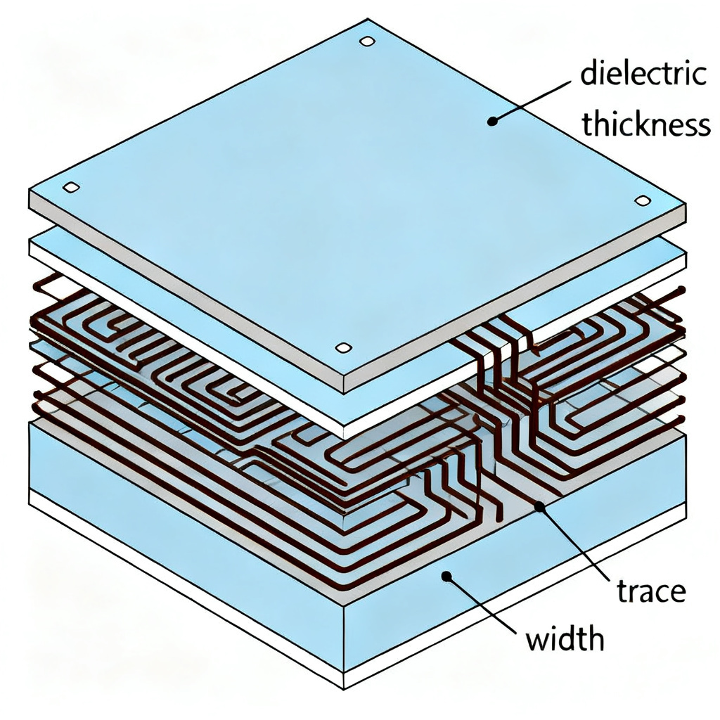
Controlled Impedance PCB Design
Work with a B2B PCB manufacturer that offers controlled impedance fabrication. Specify stackup parameters (dielectric thickness, trace width, copper weight) to achieve Z_0 within ±5% tolerance. Use microstrip or stripline configurations depending on layer count. For differential pairs (e.g., USB, HDMI), maintain differential impedance (e.g., 100Ω ±10%).
Minimize Discontinuities
- Reduce via stubs: Use back-drilling to remove unused via portions, or transition to micro-vias in HDI designs.
- Avoid sharp bends: Use 45° or curved traces instead of 90° corners to reduce impedance changes.
- Optimize connector placement: Use impedance-controlled connectors and keep trace lengths matched.
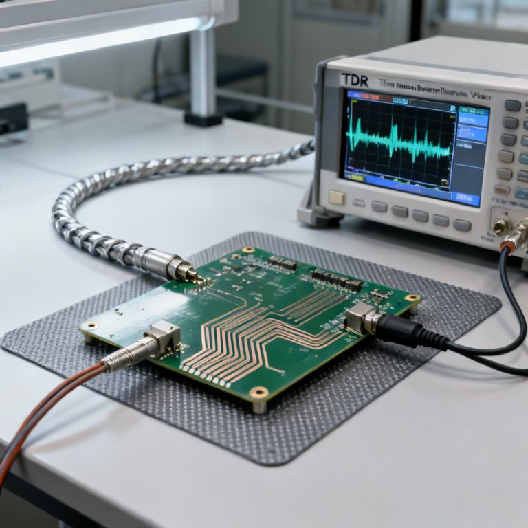
Use of Simulation Tools
Before fabrication, simulate the transmission line with tools like:
- SPICE: Model the line as a distributed RLCG network with realistic coefficients.
- IBIS models: Use driver/receiver IBIS files to predict reflections and settling time.
- 3D electromagnetic solvers: For complex geometries (e.g., BGA breakout regions), simulate full-wave effects.
Employ Termination Networks for Multi-Drop Buses
In multi-drop topologies (e.g., DDR memory bus), reflections from each load interact. Use fly-by topology with parallel termination at the far end, or source-series termination with carefully placed resistors. Avoid daisy-chain routing unless matched stubs are short.
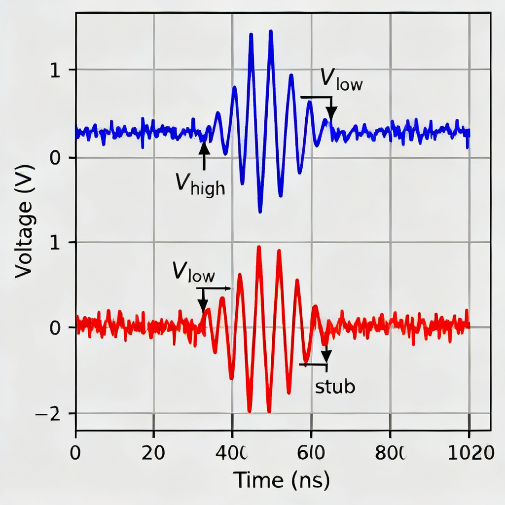
Case Study: Ringing and Settling Time in a 10 Gbps PCB
Scenario
A 10 Gbps NRZ signal (rise time = 35 ps) travels on a 50Ω microstrip line of length 15 cm (t_pd = 6 ps/mm, round-trip delay = 1.8 ns). The driver has Z_S = 15Ω, and the receiver has Z_L = 1MΩ (high impedance). Without termination:
- First reflection: Γ_L ≈ 0.96 → overshoot to 1.96× initial voltage.
- Second reflection: Γ_S ≈ -0.54 → undershoot to 0.46× initial voltage.
- Ringing frequency: ≈ 278 MHz (period = 3.6 ns).
- Settling time to ±10%: ~7 ns (4 round trips).
Mitigation
Add series termination R_S = 35Ω at the driver (total Z_S = 50Ω). This reduces Γ_S to 0, eliminating all reflections after the first. The load still sees a single reflection (overshoot), but no further ringing. Settling time drops to < 0.5 ns.
Result
The eye diagram opens from 0.4 UI to 0.8 UI, and jitter reduces by 60%. This demonstrates the critical role of termination in high-speed PCB design.
Structured Data: Key Parameters for Multiple Reflections
| Parameter | Typical Value | Impact on Multiple Reflections in Transmission Line |
|---|---|---|
| Characteristic Impedance (Z_0) | 50Ω | Mismatch creates reflections; matching reduces ringing |
| Round-Trip Delay | 1.8 ns (15 cm trace) | Longer delay increases settling time |
| Reflection Coefficient (Γ) | 0.96 (open load) | Higher Γ amplifies ringing amplitude |
| Rise Time | 35 ps (10 Gbps) | Faster rise time excites higher-frequency ringing |
| Stub Length | 1 mm | Adds 50 ps settling time increase |
FAQ: Multiple Reflections in Transmission Line
What are multiple reflections in transmission line?
Multiple reflections in transmission line occur when a signal bounces back and forth between impedance discontinuities (e.g., source and load mismatches), creating delayed voltage perturbations that cause ringing and extended settling time.
How do multiple reflections in transmission line create ringing?
Ringing results from constructive and destructive interference of multiple reflections in transmission line. When the round-trip delay exceeds the signal rise time, reflections superimpose, producing damped oscillations at the receiver.
What is settling time in the context of multiple reflections in transmission line?
Settling time is the duration for the signal to stabilize within a specified tolerance (e.g., ±10%) after an edge. Multiple reflections in transmission line prolong settling time because each reflection adds a delayed perturbation that must decay.
How can I mitigate multiple reflections in transmission line?
Mitigation includes impedance matching (series or parallel termination), controlled impedance PCB design, minimizing discontinuities (e.g., via stubs), using simulation tools, and employing termination networks for multi-drop buses.
Conclusion: Mastering Multiple Reflections for Reliable High-Speed PCB Design
Multiple reflections in transmission line are an inevitable consequence of impedance discontinuities in high-speed PCBs. They directly create ringing—characterized by voltage overshoot/undershoot and high-frequency oscillations—and prolong settling time, threatening timing margins and signal integrity. By understanding the reflection coefficient mechanism, lattice diagram analysis, and the impact of line length and rise time, engineers can predict and mitigate these effects.
For B2B PCB manufacturers, offering controlled impedance fabrication, back-drilling, and simulation support is essential to help clients achieve first-pass success. Whether designing for 1 Gbps Ethernet or 112 Gbps PAM4, the principles of impedance matching, topology optimization, and termination remain the foundation of robust high-speed design.
By mastering these concepts, you ensure that your PCB products deliver the performance, reliability, and compliance demanded by today’s high-speed digital systems.