Understanding reflection in transmission line for PCIe compliance is critical for high-speed PCB design. As PCIe data rates reach 32 GT/s, even minor impedance mismatches cause signal degradation and compliance failure. This guide defines the exact reflection limits for PCIe Gen3, Gen4, and Gen5, providing actionable design rules for engineers and manufacturers.
Reflection Limits Overview for PCIe Compliance
Reflection termination in transmission line for PCIe compliance is governed by three key metrics: differential impedance tolerance, return loss, and reflection coefficient. All three must be met to ensure signal integrity at high data rates.
Differential Impedance Tolerance for PCIe
The PCIe Base Specification mandates 85Ω differential impedance with a ±15% tolerance for Gen1 through Gen5. However, for Gen4 and Gen5, industry experts recommend ±10% or even ±5% to maintain sufficient margin against reflection-induced jitter. Single-ended traces must target 50Ω ±10%.
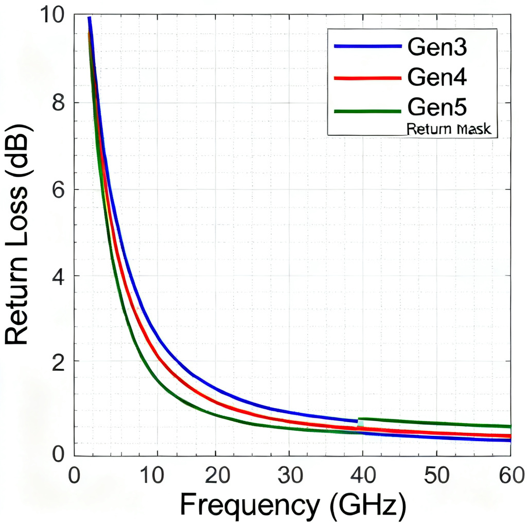
Return Loss Specifications by PCIe Generation
Return loss quantifies reflected signal power. For PCIe Gen3, return loss must be better than -10 dB from 50 MHz to 4 GHz. For Gen4, the same -10 dB limit applies up to 8 GHz. For Gen5, the requirement tightens to -12 dB up to 16 GHz. Above these frequencies, the limit relaxes to -6 dB for all generations.
Reflection Coefficient Targets
The reflection coefficient (Γ) must remain below 0.15 for Gen3 and Gen4, and below 0.10 for Gen5. This directly correlates to the return loss limits and ensures minimal signal distortion.
Sources of Reflection in PCIe Transmission Lines
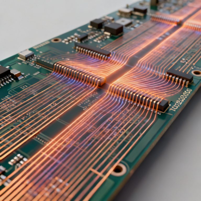
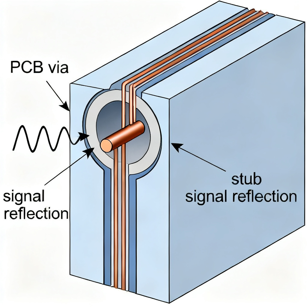
Reflection in transmission line for PCIe compliance arises from impedance discontinuities, via stubs, connector transitions, and trace geometry variations. Each source contributes to the total reflection budget.
Via Stubs and Connector Mismatches
Unused via stubs create capacitance and inductance mismatches. Back-drilling is mandatory for Gen4 and Gen5. A 20-mil stub at 16 GT/s can cause a 0.3 dB insertion loss penalty and increase reflection by 5%. Connector transitions, especially PCIe edge connectors, require impedance-controlled footprints with ground vias.
Trace Width and Dielectric Variations
PCB fabrication tolerances in trace width (±10%) and dielectric height directly affect impedance. Tightening tolerances to ±5% for high-speed layers reduces reflection. Prepreg thickness variations of 1 mil can shift impedance by 5-10Ω.
Crosstalk-Induced Reflections
Near-end and far-end crosstalk add noise that can be mistaken for reflection. PCIe compliance limits crosstalk to -30 dB or better between differential pairs. Maintain 3W spacing (three times the trace width) between PCIe lanes to minimize coupling.
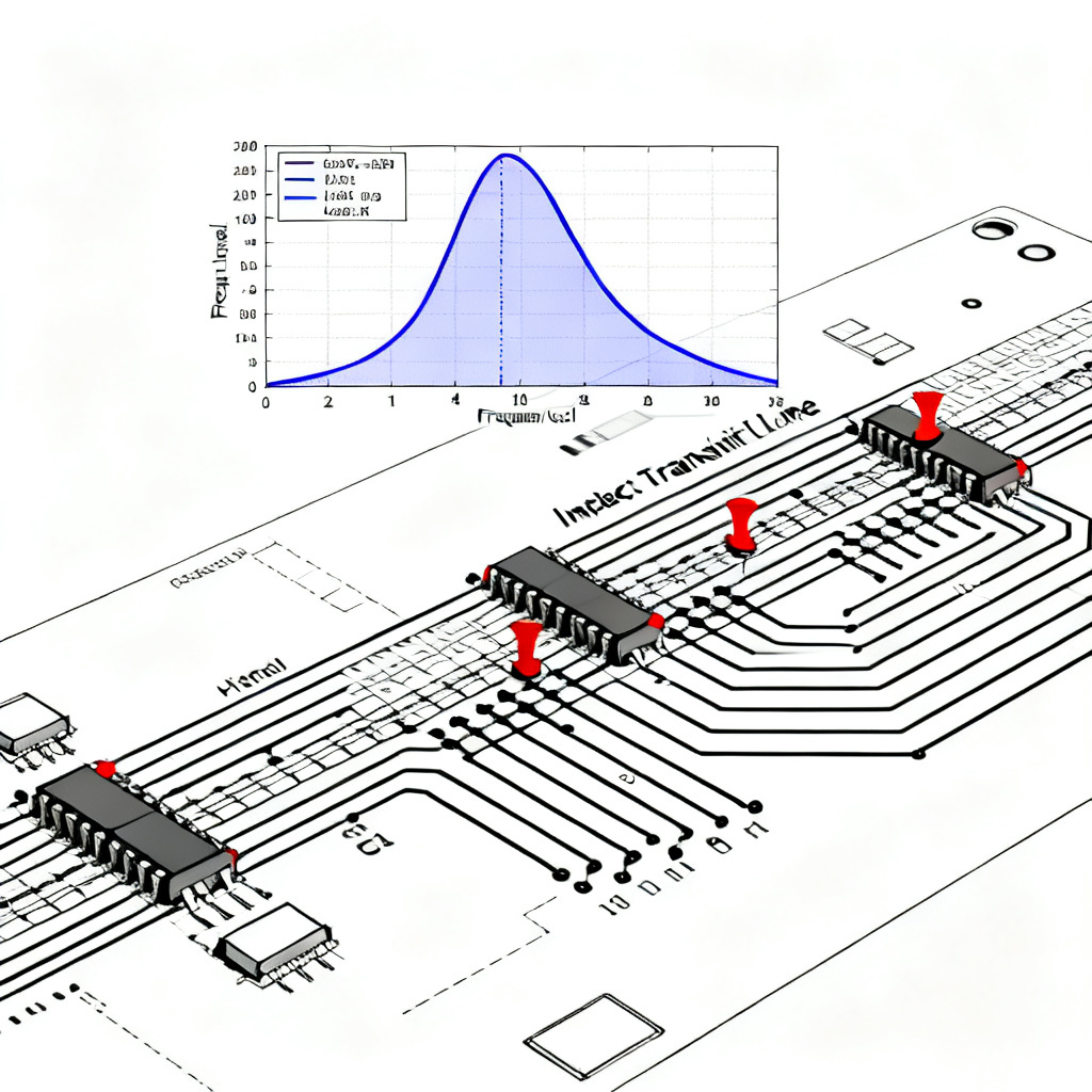
Compliance Testing Methods for Reflection Limits
Verifying reflection in transmission line for PCIe compliance requires TDR, VNA, and eye diagram testing. Each method provides a different perspective on signal integrity.
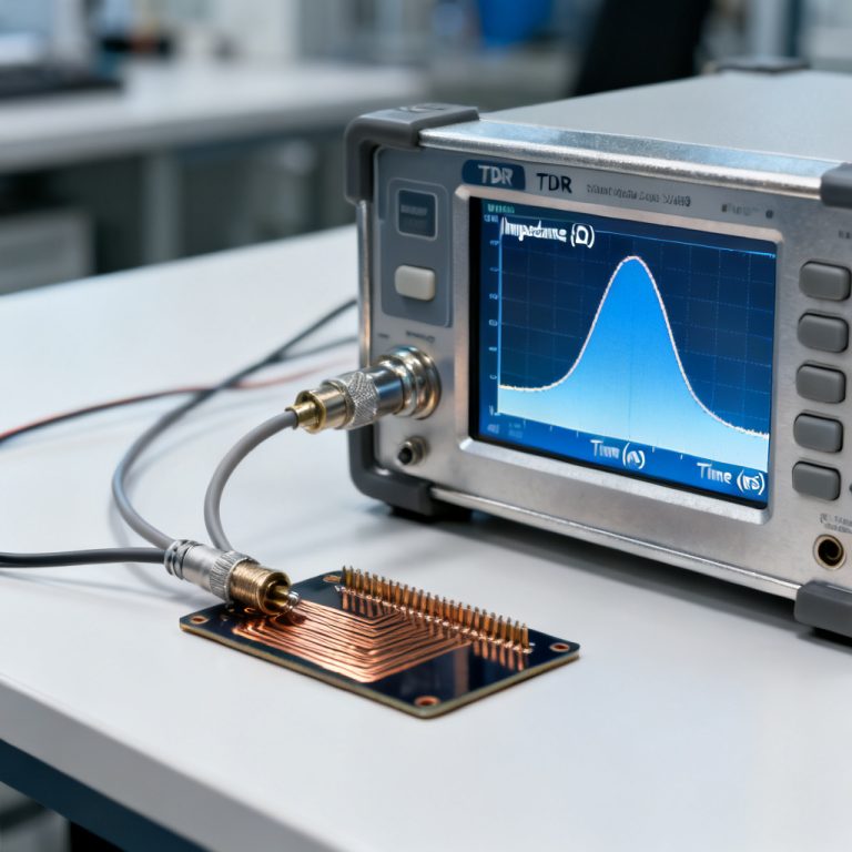
TDR Testing Procedure
Use a TDR oscilloscope with a 35 ps rise time for Gen3/Gen4 and 20 ps for Gen5. Launch a step pulse and measure reflected voltage. Impedance must stay within 85Ω ±15% for the entire trace length. For Gen5, ±10% is recommended.
VNA Testing for Return Loss
Use a 4-port VNA calibrated to 85Ω differential. Measure S11 and S22. Convert to return loss using RL = -20 log10|S11|. Compare to the frequency-dependent masks in Section 1.2.
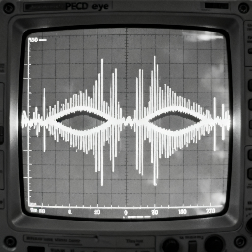
Eye Diagram Verification
Transmit a PRBS pattern and capture the eye diagram. Reflections cause eye closure. PCIe compliance requires a minimum eye opening of 0.5 UI for Gen3, 0.4 UI for Gen4, and 0.3 UI for Gen5.
Practical PCB Design Rules for Reflection Compliance
To minimize reflection in transmission line for PCIe compliance, follow these stack-up, routing, and connector design rules.
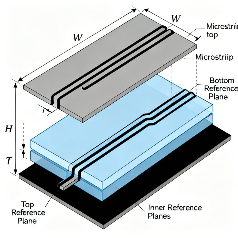
Stack-Up Design Guidelines
Use symmetrical stack-ups with an even number of layers. Every high-speed signal layer must be adjacent to a solid ground plane. Use low-loss materials like Megtron 6 or Rogers 4350B for Gen4/Gen5. FR-4 is acceptable only for Gen3 and below.
Trace Routing Best Practices
Match PCIe lane lengths within ±5 mils for Gen3 and ±2 mils for Gen4/Gen5. Avoid right-angle bends; use chamfered or curved bends. Keep differential pairs tightly coupled with a constant gap.
Connector and Footprint Optimization
Place ground vias near each signal via. For PCIe edge connectors, add ground stitching vias every 100 mils. Remove solder mask from card-edge fingers to maintain consistent impedance.
Frequency-Dependent Reflection and PCIe Speed
Reflection in transmission line for PCIe compliance becomes more critical at higher frequencies due to skin effect, dielectric loss, and quarter-wave resonance. A 10% impedance mismatch at 1 GHz causes 0.1 dB reflection loss; at 16 GHz, the same mismatch causes 0.5 dB loss. For Gen5, keep all discontinuities shorter than 0.5 mm to avoid resonance.
Common Compliance Failures and Solutions
| Failure Mode | Root Cause | Solution |
|---|---|---|
| Impedance too low (75Ω) | Trace too wide or dielectric too thin | Adjust trace width; use thicker prepreg |
| Impedance too high (95Ω) | Trace too narrow or dielectric too thick | Increase trace width; reduce dielectric height |
| Return loss fails at high frequency | Via stubs, connector mismatch | Back-drill vias; optimize connector footprint |
| Eye diagram closure | Multiple small reflections accumulate | Reduce number of vias; use smooth bends |
| Crosstalk-induced jitter | Traces too close together | Increase spacing to 5W; add guard traces |
Expert Glossary: Key Terms for Reflection in Transmission Line
Return Loss: The ratio of reflected power to incident power, expressed in dB. A higher absolute value indicates better impedance matching.
Reflection Coefficient (Γ): The ratio of reflected voltage to incident voltage. It directly measures the magnitude of impedance mismatch.
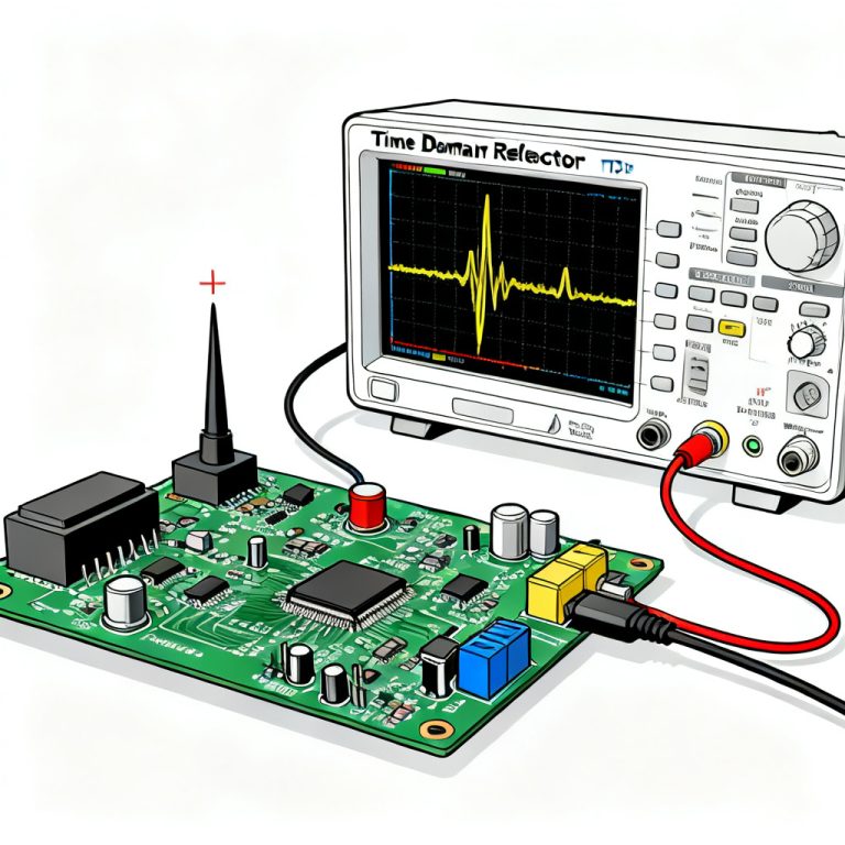
Time-Domain Reflectometry (TDR): A measurement technique that uses a fast step pulse to locate and quantify impedance discontinuities along a transmission line.
Quarter-Wave Resonance: A condition where a discontinuity length equals one-quarter of the signal wavelength, causing maximum reflection.
Why Choose Our High-Speed PCB Manufacturing
Our factory delivers ±5% impedance tolerance, back-drilling, and low-loss materials for PCIe Gen3, Gen4, and Gen5. We provide TDR and VNA test reports with every order, ensuring your reflection in transmission line for PCIe compliance is verified before assembly. Contact us for a quote with your stack-up requirements.
Frequently Asked Questions
What is the exact impedance tolerance for PCIe Gen5?
For PCIe Gen5, the reflection in transmission line for PCIe compliance requires differential impedance of 85Ω ±15% per specification, but ±10% is recommended for production margin.
How do via stubs affect PCIe compliance?
Via stubs create impedance discontinuities that increase reflection. Back-drilling is mandatory for Gen4 and Gen5 to meet return loss limits.
What testing is required for PCIe reflection compliance?
TDR, VNA, and eye diagram testing are all required. TDR measures impedance profile, VNA measures return loss, and eye diagrams verify signal quality at the receiver.
Can FR-4 meet PCIe Gen5 reflection limits?
FR-4 typically cannot meet the tight reflection and loss requirements for Gen5. Low-loss materials like Megtron 6 or Rogers 4350B are recommended.
What is the maximum allowable reflection coefficient for PCIe?
For Gen3 and Gen4, the reflection coefficient must be below 0.15. For Gen5, it must be below 0.10.